6-Pin Header Design Tutorial: HTSW-106-14-L-S PCB Layout Guide
Introduction to the Component
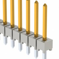
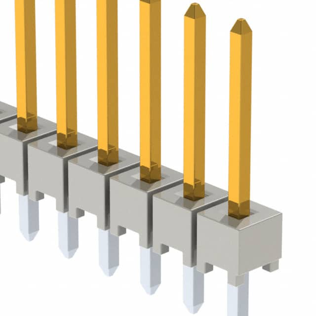
The Samtec HTSW-106-14-L-S is a 6-position, single-row, through-hole pin header with a standard 2.54mm (0.1-inch) pitch. This component is ideal for a hands-on design tutorial because it represents the most common form of interconnect in hobbyist and professional electronics: a robust, solderable connector for prototyping, modular designs, and test points. Its vertical orientation and square pins (0.025 inch square) provide excellent mechanical strength and reliable contact for repeated mating cycles. The 2.54mm pitch aligns perfectly with breadboards, perfboards, and standard DIP IC footprints, making it a universal building block. In this tutorial, you will use this header as a key interface in a practical, multi-voltage power distribution circuit.
Design Requirements and Specifications
Your goal is to design a simple, regulated power supply module that provides +5.0V and +3.3V from a 9V DC input. This circuit will be used to power a breadboarded microcontroller and sensor array. The input voltage range is 7.5V to 12V DC (unregulated). Output requirements: +5.0V at up to 500mA and +3.3V at up to 300mA. The HTSW-106-14-L-S will serve as the input power connector (pins 1 and 2 for GND and VIN) and the output connector (pins 3-6 for +5V and +3.3V outputs and their respective grounds). Key specifications: the header is rated for 3A per pin (continuous), which exceeds our needs. Contact resistance is typically 10 milliohms. The plastic housing is high-temperature LCP, suitable for wave and reflow soldering, though we will hand-solder it.
Step-by-Step Design Process with Calculations
Step 1: Regulator Selection. For the +5V rail, we need a linear regulator that can drop from 9V to 5V at 500mA. Power dissipation: (9V - 5V) 0.5A = 2W. A standard 7805 in a TO-220 package with a heatsink is appropriate. For the +3.3V rail, we will derive it from the +5V output using a low-dropout (LDO) regulator (e.g., LM1117-3.3) to minimize heat. Max dissipation: (5V - 3.3V) 0.3A = 0.51W, manageable without a heatsink.
Step 2: Input and Output Capacitors. The 7805 requires a 0.33µF input capacitor (C1) and a 0.1µF output capacitor (C2) for stability. The LM1117 requires a 10µF tantalum output capacitor (C3) for stability. Add a 100µF electrolytic capacitor (C4) on the input to smooth incoming ripple from the 9V supply.
Step 3: Header Pin Assignment. Using the HTSW-106-14-L-S (6 pins, single row), assign: Pin 1 = GND (input), Pin 2 = VIN (9V input), Pin 3 = +5V output, Pin 4 = GND (output), Pin 5 = +3.3V output, Pin 6 = GND (output). This provides a clean, modular interface. The header pins will be soldered into a perforated board with copper traces.
Step 4: Heatsink Calculation for 7805. With 2W dissipation, ambient temperature 35°C, and maximum junction temperature 125°C for the 7805, thermal resistance junction-to-ambient (RθJA) must be ≤ (125°C - 35°C) / 2W = 45°C/W. The 7805 alone has RθJA ~65°C/W, so a heatsink with RθSA ≤ 10°C/W is needed (e.g., a small clip-on finned heatsink).
Component Selection Rationale for the Complete BOM
Main Components: 7805 (TO-220) - widely available, robust, and cheap. LM1117-3.3 (SOT-223) - low dropout voltage (1.2V max) allows operation from 5V. HTSW-106-14-L-S - chosen for its high pin count (6) to accommodate all power rails on one connector, reducing wiring errors. Capacitors: 0.33µF ceramic (X7R, 50V) for C1, 0.1µF ceramic (X7R) for C2, 10µF tantalum (16V) for C3, 100µF aluminum electrolytic (25V) for C4. Tantalum is specified for the LM1117 due to low ESR requirements. Heatsink: Wakefield 6237B-MTG or equivalent clip-on type. Other: Perforated prototyping board, 22 AWG solid wire, solder, and a 9V battery clip with connector.
Simulation Tips and What to Look For
Simulate the circuit in LTspice or a similar tool. Use the 7805 and LM1117 SPICE models. Key checks: Startup behavior - ensure the +5V rail rises monotonically without oscillations. Look at the load transient response by stepping the load on the +5V output from 10mA to 500mA; the output should stabilize within a few microseconds with less than 100mV droop. For the +3.3V rail, check that it remains stable when the +5V rail is loaded. Thermal simulation is not necessary here, but you can calculate junction temperatures manually. The simulation also verifies that the input capacitor (100µF) is adequate to prevent the 7805 from dropping out during load steps.
Prototype Build and Testing Methodology
Build: 1) Cut the perforated board to a 3x4cm size. 2) Solder the HTSW-106-14-L-S header at one edge, ensuring pins align with the board holes. 3) Solder the 7805 with its heatsink attached, keeping the tab oriented for air flow. 4) Solder the LM1117-3.3 (use a small PCB adapter if using SOT-223). 5) Add capacitors C1, C2, C3, C4 as close to the regulator pins as possible. 6) Wire the input power (pins 1 and 2) to the 9V battery clip. Testing: 1) With no load, measure input voltage (should be ~9V) and output voltages (should be 5.0V ±2% and 3.3V ±2%). 2) Apply a 500mA load to the +5V output (e.g., a 10Ω, 10W resistor). Measure the voltage drop; it should be less than 100mV. Check the 7805 temperature with a thermocouple; it should be below 80°C. 3) Apply a 300mA load to the +3.3V output and verify regulation. 4) Test ripple rejection by adding a 100mV, 120Hz ripple to the input (use a signal generator and coupling capacitor). The output ripple should be less than 5mV.
Performance Verification and Optimization
Record all measurements. Compare the +5V output voltage under full load (500mA) to the no-load value. The difference should be < 50mV. For the +3.3V rail, the difference should be < 30mV. If the 7805 runs too hot (>100°C), increase the heatsink size or add a series power resistor before the 7805 to drop some voltage (e.g., a 2Ω, 5W resistor reduces dissipation by 1W). For lower output noise, add a 10µH ferrite bead in series with the +5V output and a 10µF ceramic capacitor at the output. The HTSW-106-14-L-S header allows easy reconfiguration: you can repurpose unused pins for future test points. This design is now a reliable, modular power supply module for your workbench.