Decoding the SIT3372AC Datasheet: MEMS VCXO Guide
The SiTime SIT3372AC-4B3-28NC173.370750 is a Micro-Electromechanical Systems (MEMS) based Voltage Controlled Crystal Oscillator (VCXO) that outputs a High-Speed Current Steering Logic (HCSL) signal at a precise frequency of 173.37075 MHz. This component is designed to replace traditional quartz-based VCXOs, offering superior reliability and performance in high-speed timing applications such as data centers, networking equipment, and FPGA clocking. Understanding its datasheet is crucial for proper integration.
Key Electrical Specifications and Practical Implications
The most critical parameters for this VCXO are its nominal frequency, supply voltage, and control voltage range. The part operates from a nominal 2.8V supply voltage (Vdd), which must be maintained within ±10% for guaranteed performance. The HCSL output is a differential current-steering logic, requiring 50-ohm termination to ground on each output pin, typically via an external resistor network. The absolute pull range (APR) is specified as ±50 ppm minimum, meaning the frequency can be adjusted by at least ±50 parts per million from the center frequency when the control voltage (Vc) is varied from 0V to Vdd. This control voltage has an input impedance of approximately 10-20 kΩ, so a low-impedance source is recommended to avoid loading effects. The phase jitter (12 kHz to 20 MHz integration band) is typically 0.5 ps RMS, which is excellent for 10 Gigabit Ethernet and PCIe Gen 3 applications. In practice, this low jitter ensures minimal timing errors in high-speed serial links, directly impacting bit error rates (BER).
Absolute Maximum Ratings and Derating
The datasheet specifies absolute maximum ratings that must never be exceeded, even momentarily. The supply voltage must not exceed 3.63V, and the control voltage input must stay within -0.5V to Vdd+0.5V. Exceeding these limits can cause permanent damage to the MEMS resonator or the integrated CMOS ASIC. Derating is essential for long-term reliability. For example, while the operating temperature range is -20°C to +70°C (commercial grade), continuous operation near the maximum temperature of +70°C should be avoided if possible. A common derating guideline is to reduce the maximum junction temperature by 20°C from the rated limit. Since this is a MEMS device, it is less sensitive to shock and vibration than quartz, but still, electrostatic discharge (ESD) sensitivity is a concern. The device is rated for 2 kV HBM (Human Body Model), so standard ESD precautions during handling and assembly are mandatory. The start-up time is typically 10 ms; ensure your system’s power-on reset sequence accommodates this delay before the clock is used.
Typical Application Circuit Analysis
The application circuit for the SIT3372VCXO is straightforward but requires attention to termination. The HCSL outputs (OUT and OUTB) are open-drain current sources that must be terminated with 50-ohm resistors to ground, each located as close to the receiver as possible. A common configuration uses a 100-ohm differential termination resistor between the two outputs, combined with 50-ohm pull-down resistors. For the control voltage input, a simple RC low-pass filter (e.g., 1 kΩ and 0.1 µF) is recommended to filter noise from the tuning voltage, as any ripple on Vc directly modulates the output frequency. The supply voltage should be bypassed with a 0.1 µF ceramic capacitor placed within 2 mm of the Vdd pin, plus a larger 10 µF bulk capacitor nearby. The output enable (OE) pin, if present, is typically pulled high to enable the output; leaving it floating may cause erratic behavior. Note that the control voltage range is ratiometric to Vdd; if Vdd is 2.8V, a Vc of 0V gives the lowest frequency, while 2.8V gives the highest. For optimal phase noise, ensure the Vc source has minimal noise, ideally below 1 µVrms in the 12 kHz to 20 MHz band.
Pin Configuration and Package Considerations
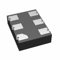
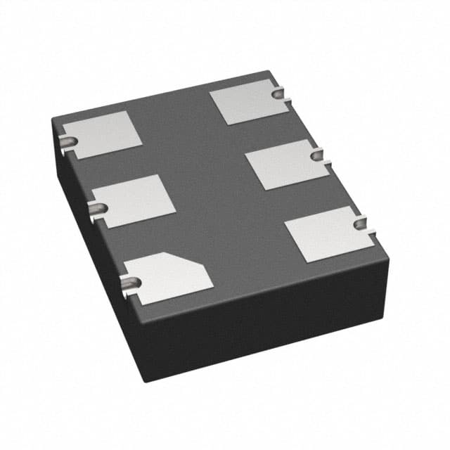
The device comes in a 6-pin or 4-pin package, typically a 3.2 x 2.5 mm QFN or similar. The pinout includes Vdd, GND, OUT, OUTB, Vc, and OE (or NC). The package has an exposed pad on the bottom that must be soldered to a ground plane for proper thermal and electrical performance. This pad provides a low-inductance ground return, which is critical for maintaining signal integrity at 173 MHz. When laying out the PCB, keep the differential output traces matched in length to within 5 mils to minimize skew. The impedance of each trace should be 50 ohms to ground. Avoid routing the Vc trace near noisy digital signals, as capacitive coupling can introduce jitter. The reflow profile must follow JEDEC standards, with a peak temperature of 260°C for lead-free soldering, but the device should not be subjected to multiple reflow cycles without cooling.
Thermal Management Guidelines
Despite being a low-power device (typically 50 mA at 2.8V, so 140 mW), thermal management is still important for jitter performance. The MEMS resonator itself is temperature-compensated, but the internal ASIC generates heat. The junction-to-ambient thermal resistance (θJA) is typically 80°C/W for the QFN package on a standard PCB. With a 140 mW power dissipation, the junction temperature rise is about 11°C above ambient. In a 70°C ambient environment, the junction reaches 81°C, which is well within the 125°C maximum. However, if the device is placed near hot components or in a confined enclosure, derate the maximum ambient temperature by 10°C to maintain reliability. Ensure adequate copper pours on the PCB layers to act as a heatsink, and include thermal vias under the exposed pad to transfer heat to the ground plane.
Interpreting Timing Diagrams and Characteristic Curves
The datasheet includes several key graphs. The frequency vs. control voltage curve is a monotonic, nearly linear transfer function, typically with a slope of about 30 ppm/V. This linearity is critical for PLL (Phase-Locked Loop) loop stability. The phase noise plot shows a typical noise floor of -150 dBc/Hz at 10 kHz offset, degrading to -130 dBc/Hz at 1 kHz offset. For jitter calculations, integrate this noise over your application’s bandwidth. The start-up timing diagram shows that after Vdd reaches 90% of nominal, the output is stable within 10 ms. There may also be a frequency vs. temperature curve showing a nearly flat response, with a total deviation of ±25 ppm over the operating range. When interpreting these curves, always use the typical values for initial design, but verify against the min/max limits for worst-case analysis. For example, the APR is guaranteed at ±50 ppm, but the typical curve might show ±55 ppm; rely on the guaranteed spec for margin calculations.