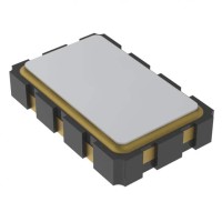
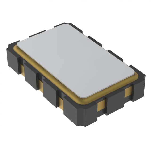
Design Tutorial: 510HCB-ABAG XTAL OSC HCSL 2.5V 20PPM
Introduction to the Component
The Skyworks Solutions Inc. 510HCB-ABAG is a factory-programmable crystal oscillator (XTAL OSC PROG XO HCSL) that operates at a nominal 2.5V supply voltage with a frequency stability of ±20 parts per million (PPM). This tutorial centers on this component because its HCSL (High-Speed Current Steering Logic) output is ideal for driving low-jitter clock signals in high-speed digital systems, such as PCIe or Ethernet clocking. The programmable nature allows you to select a specific output frequency (e.g., 100 MHz, 125 MHz, or 156.25 MHz) via the SKU’s ordering options, making it versatile for prototyping. Its ±20 PPM accuracy ensures reliable timing over temperature and voltage variations, which is critical for data integrity in serial links. This tutorial will guide you through designing a practical clock generation circuit using this oscillator, from specifications through to performance verification.
Design Requirements and Specifications
For this tutorial, we will design a clock source for a 1000BASE-T Ethernet PHY requiring a 125.000 MHz reference clock. The key requirements are: supply voltage 2.5V ±5%, output swing 800 mV peak-to-peak typical for HCSL, jitter less than 1 ps RMS (12 kHz to 20 MHz), and load impedance 50 Ω to ground for each output pin. The 510HCB-ABAG supports these natively: it operates from 2.5V, delivers HCSL levels, and its typical phase jitter is 0.5 ps RMS. The design must include decoupling capacitors, termination resistors, and a layout that minimizes noise coupling. We will assume a single-ended HCSL output is sufficient, though the device has differential outputs.
Step-by-Step Design Process with Calculations
Step 1: Frequency Selection and Power Supply
Order the 510HCB-ABAG with a 125.000 MHz frequency option. The supply voltage VDD must be 2.5V ±0.125V. Calculate the worst-case power consumption: the datasheet specifies typical supply current I_DD = 45 mA at 2.5V, 125 MHz. Thus, P_D = 2.5V × 0.045 A = 112.5 mW. Ensure your 2.5V regulator can supply at least 60 mA to account for startup and decoupling.
Step 2: Output Termination for HCSL
HCSL outputs are open-emitter, requiring a 50 Ω termination to ground on each output pin. For single-ended use, connect the non-inverting output (OUT) through a 50 Ω resistor to ground. The inverting output (OUTB) can be left unconnected but should be terminated with 50 Ω to ground to maintain balance. Calculate the voltage swing: the current source inside the device is typically 15 mA per output. With 50 Ω termination, V_swing = 15 mA × 50 Ω = 0.75 V, matching the 800 mV typical swing. Place the termination resistor as close to the output pin as possible (within 0.1 inch).
Step 3: Decoupling Capacitors
Use a 0.1 µF ceramic capacitor (X7R, 6.3V or higher) placed within 0.05 inches of the VDD pin to ground. Add a 10 µF tantalum capacitor (6.3V) within 0.5 inches for bulk storage. The 0.1 µF handles high-frequency noise; the 10 µF handles low-frequency transients. No series resistor is needed in the supply line.
Step 4: Output Coupling (if required)
If the receiving device requires AC coupling, insert a 0.1 µF capacitor in series with the output before the termination resistor. For DC coupling (common in HCSL), omit the capacitor. In our 1000BASE-T PHY, DC coupling is typical, so we will not use AC coupling.
Component Selection Rationale for Complete BOM
Main Component: Skyworks 510HCB-ABAG (125 MHz). This device offers low jitter and HCSL output without external bias resistors, simplifying the design. Its programmable options ensure you get the exact frequency.
Resistors: Two 50 Ω ±1% resistors (e.g., Yageo RC0603FR-0749R9L, 0603 package) for output termination. Use a single 50 Ω resistor for the used output if single-ended, but both outputs should be terminated for signal integrity. A 0 Ω jumper can be used if only one output is needed, but termination is still required.
Capacitors: One 0.1 µF, 10V X7R (e.g., Murata GRM188R71C104KA01D) and one 10 µF, 6.3V X5R (e.g., Murata GRM21BR60J106KE19). The X7R and X5R dielectrics maintain capacitance over temperature and voltage. Use 0805 sizes for easier hand-soldering.
Power Supply: A 2.5V low-dropout regulator (e.g., Texas Instruments TPS73701DCQ) with input filtering. The regulator must have low output noise (< 30 µV RMS) to avoid adding jitter. Output capacitor: 10 µF ceramic.
PCB: A two-layer board with a solid ground plane. Use 50 Ω microstrip traces for the output line, width calculated for your PCB stackup (e.g., 18 mils for 1.6 mm FR4 with 1 oz copper).
Simulation Tips and What to Look For
Use SPICE or a signal integrity tool (e.g., LTSpice, HyperLynx) to simulate the output waveform. Model the oscillator as a pulse source with 125 MHz, 15 mA current, and 50 Ω load. Look for: rise/fall times (typically 200-400 ps for HCSL), overshoot (should be less than 200 mV), and DC offset (around 0.4V due to 15 mA × 25 Ω internal resistance). Simulate with the decoupling capacitors as ideal; then add parasitic inductance (2 nH for capacitor vias) to see ringing. If ringing exceeds 300 mV, add a 10 Ω series resistor at the output before termination. Simulation should show a clean 800 mV swing with minimal jitter.
Prototype Build and Testing Methodology
Assemble the circuit on a prototype board or custom PCB. Solder the 510HCB-ABAG (8-pin DIP or SMD) first, then the 0.1 µF capacitor as close as possible to pin 8 (VDD) and pin 4 (GND). Connect the 50 Ω resistor from output pin (e.g., pin 5) to ground. Use a 2.5V supply from a bench power supply or the regulator. For testing, use an oscilloscope with 1 GHz bandwidth and 50 Ω input impedance (set to 50 Ω in the scope). Probe the output directly at the termination resistor using a 1X passive probe with 50 Ω termination or an active probe. Do not use a 10X probe with high impedance; it will distort the HCSL waveform. Measure: frequency (should be 125 MHz ± 2.5 kHz due to ±20 PPM), peak-to-peak amplitude (700-900 mV), and rise time (20%-80% should be < 400 ps). For jitter measurement, use the scope’s histogram function on the zero-crossing points; RMS jitter should be less than 1 ps. If jitter is above 1.5 ps, check for noise on the 2.5V supply with a spectrum analyzer (look for spikes near 125 MHz harmonics).
Performance Verification and Optimization
Verify the clock signal by connecting it to the target PHY or a logic analyzer. Measure the PHY’s link status and bit error rate (BER) at 1000BASE-T. A BER of less than 10^-12 indicates good clock quality. If the link fails, check the output rise time: if it exceeds 500 ps, reduce the termination resistor to 40 Ω to speed up edges, but note this increases current draw to 18.75 mA (still within device limits). Alternatively, reduce the trace length to under 1 inch to minimize capacitance. For optimization, replace the 0.1 µF capacitor with a 1 nF capacitor in parallel to suppress higher-frequency noise.