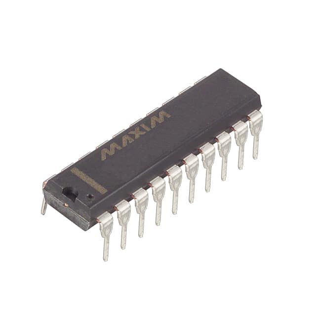
MAX186DCPP+ Application Guide: 12-Bit ADC Design Tips
The MAX186DCPP+ from Analog Devices Inc./Maxim Integrated is a 12-bit data acquisition system (DAS) integrating a successive-approximation ADC, a 4-channel multiplexer, a track/hold, and a serial interface in a 20-pin DIP package, operating at a maximum throughput of 133 kSPS. For reliable performance, begin with the recommended application circuit from the datasheet, which includes a 0.1 µF ceramic capacitor placed as close as possible to the VDD pin and a 10 µF tantalum or electrolytic capacitor in parallel for bulk decoupling. The analog input range is set by the REF pin; for a standard 0 to +5V input, connect REF to VDD through a 10kΩ resistor and bypass it with a 4.7 µF capacitor to ground. For bipolar inputs, use an external precision reference like the MAX6341. Always drive the analog inputs from a low-impedance source (< 1kΩ) to avoid sample-and-hold errors; if the source impedance is higher, buffer with a unity-gain op-amp such as the MAX4162. The serial interface (SCLK, DIN, DOUT) requires pull-up resistors if connected to open-drain logic, but since this device uses CMOS levels, direct connection to a microcontroller is sufficient. Ensure the chip-select (CS) signal is held low during the entire conversion to prevent data corruption.
Component selection for supporting passives is critical to achieving the full 12-bit accuracy. For the reference bypass capacitor, use a low-ESR ceramic type (X7R or C0G dielectric) with a tolerance of 10% or better; excessive ESR can introduce noise and drift. The analog input filter capacitor, if used, should be a film or C0G type to minimize dielectric absorption, as standard X7R capacitors can cause linearity errors due to voltage coefficient. For the serial interface, limit series resistors to 100Ω or less to avoid slowing the SCLK rise time below the 50 ns minimum requirement. The power supply decoupling network must include a 1µF to 10µF electrolytic capacitor in parallel with a 0.1µF ceramic; the electrolytic should have an ESR below 1Ω to handle transient loads from the ADC’s internal charge pump. Avoid using capacitors with high leakage current (e.g., tantalum at high temperatures) near the REF pin, as leakage can shift the reference voltage and degrade accuracy.
PCB layout is paramount for this mixed-signal device. Place the MAX186DCPP+ on a dedicated analog ground plane, separate from the digital ground plane, and connect them at a single point (often the ADC’s ground pin) using a ferrite bead or a 0Ω resistor bridge. Keep the analog input traces as short as possible and route them away from digital signal lines (SCLK, DIN, DOUT) by at least 3 mm to reduce crosstalk. The reference bypass capacitor must be placed within 5 mm of the REF pin, with a direct via to the analog ground plane. Use a solid ground fill under the IC to minimize inductance; avoid splitting the ground plane under the ADC. For the serial interface, route SCLK as a clean clock line with a 50 Ω series termination resistor at the source to suppress reflections if the trace length exceeds 2 inches. Do not run the SCLK trace parallel to analog input traces for more than 1 cm. The power supply trace should be at least 20 mils wide to handle the 2 mA typical current, and include a ferrite bead (e.g., 100Ω at 100 MHz) in series with the VDD line if the supply is noisy.
EMC/EMI considerations begin with the ADC’s high-impedance analog inputs being sensitive to RF interference. Add a 100 pF to 220 pF capacitor from each analog input to analog ground, placed as close to the IC pin as possible, to shunt high-frequency noise. For the serial interface, use a common-mode choke on the SCLK and DOUT lines if the cable length exceeds 10 cm, but this is rarely needed for on-board routing. The entire analog section should be shielded by a grounded copper pour on the top layer, connected to the analog ground plane with stitching vias every 5 mm. Avoid creating ground loops by ensuring that the analog and digital grounds are only connected at the star point. If the system includes a switching power supply, add a 1 µH inductor in series with the VDD line after the decoupling capacitors to filter ripple. For radiated emissions, keep the SCLK frequency below 10 MHz if possible; the MAX186’s maximum SCLK is 2.5 MHz at 133 kSPS, which is benign for most designs.
Common design pitfalls include neglecting the track/hold settling time—the input should be stable for at least 1 µs before the start of conversion, or you risk missing code errors. Another frequent issue is using the internal reference without adequate bypassing; a 4.7 µF capacitor is mandatory, but if the reference voltage drifts, consider an external reference like the MAX873. The serial interface can be corrupted by floating inputs: always drive CS, SCLK, and DIN to a known state when not in use, or use pull-down resistors (10kΩ) to ground. Also, never exceed the absolute maximum ratings on the analog inputs—VIN must stay within -0.3V to VDD+0.3V. A subtle trap is the power-up sequence: ensure VDD is stable before applying analog signals, or use a 1kΩ series resistor on the analog inputs to limit inrush current. Finally, do not attempt to read data during a conversion; the DOUT pin is tristated until the conversion is complete, and reading it early will yield garbage.
For prototyping, solder the MAX186DCPP+ onto a perfboard with a ground plane layer if possible, using a socket for easy replacement. Power the board with a clean linear supply (e.g., a 5V bench supply) to avoid line noise during initial tests. Use a function generator with a 50Ω output to drive the analog inputs, but add a 10kΩ series resistor at the ADC input to limit current if the generator glitches. For bench testing, start with a known DC voltage (e.g., 1.25V from a reference) and verify the output code using a logic analyzer or a microcontroller reading the serial data. Check the SCLK waveform with an oscilloscope to ensure it meets the 50 ns minimum high/low time and has clean edges (rise time < 20 ns). If the readings are noisy, add a 10 nF capacitor from the analog input to ground and re-test. Calibrate the system by recording the output for 0V and 5V inputs, then verifying linearity at mid-scale (2.5V). Use a 1 kHz sine wave to test dynamic performance; the output should show no missing codes and a signal-to-noise ratio close to 72 dB for a 12-bit system. If you see erratic readings, check for ground loops by lifting the oscilloscope ground clip and using a differential probe instead.
IC DAS/ADC 12BIT 133K 20DIP
Analog Devices Inc./Maxim Integrated | MAX186DCPP+ | $36.10