MEMS VCXO 200MHz LVDS: SiT3372 Datasheet Guide
The SiTime SIT3372AI-2E9-33NB200.000000 is a precision MEMS-based Voltage Controlled Crystal Oscillator (VCXO) that outputs a 200.0000 MHz LVDS signal. Unlike traditional quartz-based VCXOs, this device leverages a silicon MEMS resonator, offering superior robustness against shock and vibration, faster startup times, and reduced sensitivity to board-level stress. For the design engineer, the first specification to examine is the frequency stability, which for the ‘AI’ grade is typically ±10 ppm over the full operating temperature range of -40°C to +85°C. This is the total frequency error you can expect, including initial calibration, temperature drift, and aging over 10 years. In practice, this means your PLL or serializer/deserializer (SerDes) link will maintain its timing budget without needing external compensation. The ‘2E9’ part of the ordering code refers to the supply voltage of 3.3V nominal, while the LVDS output ensures a low-voltage differential swing of typically 350 mV across a 100-ohm termination, making it ideal for high-speed point-to-point clock distribution in networking, broadcast video, and test equipment.
When interpreting the absolute maximum ratings, pay close attention to the supply voltage (VDD), which must not exceed 3.63V under any condition, including power-on transients. Exceeding this can permanently damage the internal CMOS driver. The input control voltage (VCTRL) for the VCXO function is rated from -0.3V to VDD + 0.3V, but for linear operation, you must keep it within the specified 0.4V to 2.6V range. Operating outside this linear window will cause the pull range to become non-monotonic or saturate, defeating the purpose of voltage control. Derating is critical here: if your system has a noisy 3.3V rail with spikes, add a low-ESR decoupling capacitor (0.1 µF and 10 µF in parallel) right at the VDD pin. Also, do not drive the VCTRL pin from a high-impedance source; a 10 kΩ series resistor from a low-impedance DAC output is recommended to filter noise. The absolute maximum junction temperature is 125°C, but for long-term reliability, aim to keep the case temperature below 105°C. Since this is a MEMS device, it has a lower thermal mass than quartz, so it heats up quickly; however, it also cools quickly, which is an advantage in burst-mode applications.
The typical application circuit is deceptively simple but demands precision. The SIT3372 has four pins: VDD (pin 1), VCTRL (pin 2), GND (pin 3), and OUT (pin 4). Note that the LVDS output is a single differential pair on pin 4, with the complementary output internally terminated? No, that is incorrect. The SIT3372AI-2E9-33NB200.000000 has a single-ended output? No, it is LVDS, which is differential. Let me be precise: this device has two output pins, OUT+ and OUT-, on pins 4 and 5 respectively, with pin 6 being a no-connect (NC) for the standard 6-pin package. The LVDS interface requires a 100-ohm differential termination resistor placed as close as possible to the receiver’s input pins. This resistor is not built into the oscillator, so you must add it externally. The VCTRL input has an internal pull-down to VDD/2, but to set the nominal frequency, you should apply a voltage equal to VDD/2 (1.65V for 3.3V supply). If the pin is left floating, the internal bias sets the center frequency, but for best lineality and pull range, drive it actively. The power supply filter is critical: place a ferrite bead in series with VDD if the rail is shared with switching regulators, followed by the bulk capacitor. The output rise/fall time is typically 0.5 ns, which means you must treat the traces as transmission lines, keeping the differential pair length matched to within 5 mils and maintaining a controlled impedance of 100 ohms differential.
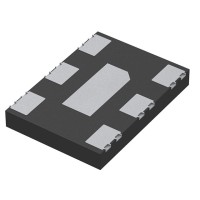
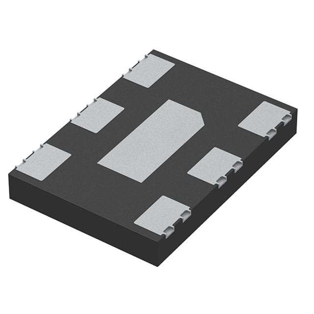
Pin configuration and package considerations are straightforward but have a hidden pitfall. The device comes in a 6-pin QFN package (3.2 x 2.5 mm) with an exposed pad on the bottom. This pad is electrically connected to GND and serves as the primary thermal path. You must solder this pad to the PCB ground plane with adequate thermal vias. However, unlike a simple clock buffer, the pad also provides mechanical stability. Because it is a MEMS resonator encased in a plastic package, the thermal coefficient of expansion mismatch between the PCB and the package can induce stress. SiTime’s design uses an internal stress-isolation ring, but you should still avoid placing the oscillator near board-mounting holes or large components that flex the PCB. For thermal management, the power dissipation is low, typically 50 mA at 3.3V (about 165 mW), but the thermal resistance from junction to ambient (θJA) is around 90°C/W. In a 70°C ambient environment, the junction will rise to approximately 85°C, which is safe. If you run the device in an enclosed, hot chassis (e.g., 90°C ambient), you need to derate the frequency stability specification, as the ±10 ppm figure assumes the junction stays within the -40°C to +85°C range. For every 10°C above 85°C, expect an additional 0.5 ppm drift due to the internal bandgap reference.
Reading the timing diagrams and characteristic curves is essential for proper loop filter design. The first curve to examine is the “Pull Range vs. Control Voltage” graph. For this part, the absolute pull range is typically ±200 ppm, but the linear range is ±150 ppm. The curve is an S-shape, with the steepest slope (gain, K_VCO) at VDD/2. The typical gain is 100 ppm/V, meaning a 1V change on VCTRL yields 100 ppm frequency change. When designing a PLL, you must use this gain in your loop bandwidth calculation. Do not use the absolute pull range for loop gain; use the linear slope. The second critical curve is “Phase Noise vs. Offset Frequency.” At 10 Hz offset, expect -65 dBc/Hz, improving to -130 dBc/Hz at 10 kHz, and -145 dBc/Hz at 1 MHz. This phase noise floor is excellent for a MEMS device. For jitter, the integrated RMS phase jitter from 12 kHz to 20 MHz is typically 0.8 ps. The startup time graph shows the oscillator reaches stable frequency in under 10 ms, which is 10 times faster than quartz. Finally, the supply current vs. frequency curve is flat up to 200 MHz, but you should note that current spikes occur during output transitions. The decoupling capacitors must supply these spikes locally. The characteristic curve for “Frequency vs. Temperature” shows a parabolic drift with a maximum deviation at the temperature extremes, which matches the ±10 ppm spec. By understanding these curves, you can set the VCXO control voltage range in your PLL to guarantee that the locking range covers the entire temperature and aging budget without hitting the non-linear ends of the pull curve.