SK24F Schottky Diode Datasheet: 40V 2A SMBF Guide
The SK24F from Panjit International is a 40-volt, 2-ampere Schottky barrier rectifier housed in the compact SMBF (SMB Flat) package. At its core, this component leverages the metal-semiconductor junction to achieve a significantly lower forward voltage drop compared to standard PN-junction diodes. For a 2A device, the forward voltage (VF) is typically specified at 0.50V maximum at 2A, which translates directly into reduced power dissipation and higher efficiency in low-voltage, high-frequency applications. This low VF is the primary reason to choose this part over a generic rectifier; in a 5V output power supply, a 0.5V drop represents a 10% loss, whereas a standard diode at 0.9V would represent an 18% loss. Furthermore, the Schottky's majority-carrier conduction mechanism eliminates minority-carrier storage time, enabling fast switching with a reverse recovery time (trr) of typically less than 10 nanoseconds. This makes the SK24F ideal for switch-mode power supplies (SMPS), DC-DC converters, and freewheeling diodes in circuits operating at frequencies from 100 kHz to over 1 MHz.
Interpreting the absolute maximum ratings is critical for reliability. The repetitive peak reverse voltage (VRRM) is 40V, but this is not a continuous operating voltage. In practice, you must ensure that the maximum reverse voltage across the diode, including any transient spikes and ringing, never exceeds this value. A common derating guideline is to operate at no more than 80% of the rated VRRM, i.e., 32V, to provide a safety margin against line surges and inductive spikes. The average forward rectified current (IO) is 2A, but this rating assumes a specific mounting condition (e.g., a 10mm x 10mm copper pad on a PCB) and a particular lead temperature (usually 75°C). If your ambient temperature is higher, you must derate the current linearly. The datasheet provides a derating curve, typically showing that at an ambient temperature of 100°C, the allowable forward current may drop to 1.2A or less. Similarly, the non-repetitive peak forward surge current (IFSM) is high, often around 50A for a single 8.3ms half-sine wave, but this is for inrush current events like capacitor charging at power-on, not for continuous operation.
In a typical application, such as a synchronous rectifier or output rectifier in a buck converter, the SK24F is placed in series with the inductor and the load. The cathode connects to the positive output rail, and the anode connects to the switching node. When the main switch turns off, the inductor forces current to flow through the diode to maintain continuity. The low VF minimizes conduction losses, while the fast recovery ensures that the diode does not conduct during the switch's off-state, preventing shoot-through currents. For a flyback converter, the diode is placed across the transformer's secondary winding to rectify the output. In both cases, a critical design consideration is the parasitic inductance of the PCB traces. The SMBF package has very low lead inductance (around 2-4 nH), but you should still place the diode close to the transformer or switch node to minimize ringing. A snubber circuit (a resistor and capacitor in series) across the diode may be necessary to damp high-frequency oscillations caused by the diode's junction capacitance (CT, typically around 150 pF at 4V reverse bias) interacting with the leakage inductance.
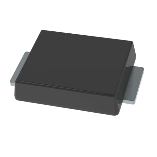
The pin configuration is straightforward: the SMBF package has two terminals, with the cathode marked by a white band on the body. The SMBF is a surface-mount package, smaller and lower-profile than the standard SMB (DO-214AA), which is beneficial for high-density designs. However, the smaller body and exposed pad mean that heat dissipation is entirely dependent on the PCB copper area. The thermal resistance from junction to ambient (RθJA) is typically around 80°C/W when mounted on a standard FR-4 board with minimal copper. This is significantly higher than a through-hole package. To manage thermal performance, you must dedicate sufficient copper area to the anode and cathode pads. A recommended layout involves a 5mm x 5mm copper pad on each terminal, connected to a larger ground plane if possible. For every additional 1W of power dissipated, the junction temperature (TJ) rises by the product of RθJA and the power. If you are dissipating 1W (which occurs at 2A forward current with a 0.5V drop), the junction will rise 80°C above ambient. With a maximum junction temperature (TJ,max) of 150°C, this limits the maximum ambient to 70°C. Therefore, for high-current applications, it is often necessary to use the diode at a reduced current (e.g., 1.5A) or increase the copper area to lower RθJA to around 60°C/W.
When interpreting the characteristic curves, focus on three graphs. The first is the forward voltage vs. forward current curve, which is logarithmic. At low currents (10 mA), VF might be only 0.2V, but at 2A, it rises to 0.5V. This curve is also temperature-dependent; VF decreases with increasing temperature (negative temperature coefficient), which can lead to thermal runaway if two diodes are paralleled without current sharing resistors. The second critical graph is the junction capacitance vs. reverse voltage curve. As VR increases from 0V to 40V, CT drops dramatically from around 250 pF to less than 50 pF. This is important for high-frequency designs because a larger capacitance at low reverse voltage causes switching losses. The third graph is the derating curve, which plots average forward current vs. ambient temperature. This curve is the most conservative; it assumes a continuous DC current, not pulsed. For pulsed operation with a low duty cycle, you can use the peak current rating (IFSM) and the thermal impedance (ZθJA) to estimate the junction temperature rise during the pulse, allowing you to exceed the average current rating safely. Always remember that the transient thermal impedance is lower than the steady-state value, so brief pulses of 5A are acceptable, but the average power must remain within the derating limits.