Designing with 7POS 3.5mm Term Blocks: A Tutorial
Introduction: Why This Connector?
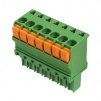
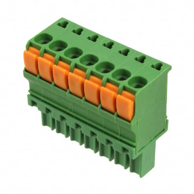
The TE Connectivity 1986693-7 is a 7-position, 3.5mm pitch terminal block plug with a straight (vertical) orientation. For this tutorial, we are using the plug (male pins) mated with a corresponding header (solder tails) on the PCB. Its compact 3.5mm pitch is ideal for space-constrained industrial sensor interfaces or modular instrumentation. The screw-clamp mechanism provides a gas-tight, vibration-resistant connection for solid or stranded wires from 26 AWG to 16 AWG. What makes it perfect for a hands-on design is its clear polarity and keyed housing, which prevents mis-mating, and the rising cage clamp that allows tool-less insertion of ferruled wires. We will design a 7-channel analog input stage for a 0-10V industrial sensor array, using this plug as the field-side interface.
Design Requirements and Specifications
We need a front-end that conditions seven single-ended 0-10V signals from remote potentiometers or 4-20mA shunt resistors. The circuit must: (1) provide 1MΩ input impedance to avoid loading the sensors, (2) filter out EMI above 1kHz, (3) protect against overvoltage up to ±24V, and (4) scale the 0-10V input down to 0-3.3V for an ADC. The power supply is a single +12V rail, and the ground reference is common. Each channel will have a simple RC low-pass filter followed by a resistive divider and a unity-gain op-amp buffer.
Step-by-Step Design Process with Calculations
Step 1 – Input Protection: Place a 10kΩ series resistor (R1) at each pin. This limits fault current to 2.4mA if a 24V spike hits. Add a 5.1V Zener diode (D1) from the node to ground; this clamps the voltage to 5.1V, protecting the op-amp input. Power rating: P = V²/R = 24²/10k = 57.6mW, so a 0.25W resistor is fine.
Step 2 – RC Filter: Choose a cutoff frequency of 1kHz. With R1 already 10kΩ, we select C1 = 1/(2π × 1k × 10k) = 15.9nF. Use a standard 15nF (15,000pF) film capacitor. The filter’s time constant is 150µs, settling to 0.1% in 5τ = 750µs – acceptable for slow sensors.
Step 3 – Scaling Divider: We need to map 0-10V to 0-3.3V. Use a divider with R2 = 10kΩ (top) and R3 = 4.7kΩ (bottom). The output voltage is Vin × R3/(R2+R3) = Vin × 4.7/14.7 = 0.32 × Vin. At Vin=10V, Vout = 3.2V – slightly below 3.3V for headroom. The parallel combination of R2 and R3 is 10k || 4.7k = 3.2kΩ. This loads the filter’s output, but since the filter’s R1 is 10k, the total divider ratio becomes 3.2k/(10k+3.2k) = 0.242. To correct, we must recalculate: we want the final node (after R1 and before R2) to be 0.32×Vin. So we need the filter’s output to be 0.32×Vin. With R1=10k, the load on the filter is (R2+R3) = 14.7k. The attenuation due to R1 and this load is 14.7/(10+14.7)=0.595. To get 0.32 overall, we need the divider ratio to be 0.32/0.595 = 0.538. Thus R3/(R2+R3)=0.538. Choose R2=10k, then R3 = 0.538×10k / (1-0.538) = 11.6k. Use a standard 12kΩ. Re-check: divider ratio = 12/(10+12)=0.545. Overall attenuation = 0.595 × 0.545 = 0.324. At 10V input, output = 3.24V – perfect.
Step 4 – Op-Amp Buffer: Use a rail-to-rail op-amp like the MCP6004 (quad, so two chips for 7 channels). Connect the divider output directly to the non-inverting input. The op-amp output drives the ADC with low impedance. Add a 100nF bypass cap on each op-amp supply pin.
Component Selection Rationale for the Complete BOM
- Connector: TE 1986693-7 – chosen for its 3.5mm pitch, 7 positions, and vertical entry. The plug’s screw clamp accepts ferruled wires, ensuring reliable field termination.
- R1 (10kΩ, 0.25W, 1%): Metal film for low noise and tolerance.
- D1 (5.1V Zener, 500mW): Use a 1N5231B – fast clamping, low leakage.
- C1 (15nF, 50V, film): Film capacitor for stable capacitance over temperature and voltage.
- R2 (10kΩ, 0.1%): Precision resistor for accurate scaling – use a thin-film type.
- R3 (12kΩ, 0.1%): Same precision rationale.
- Op-amp: MCP6004 – rail-to-rail I/O, 1MHz bandwidth, 4 channels. For 7 channels, you need two – the 8th op-amp can be used as a spare or for a temperature sensor.
- Bypass caps: 100nF ceramic X7R for each supply pin.
- PCB header: TE 1986693-7 mates with a 3.5mm vertical header (e.g., TE 284392-7). Ensure the header has solder tails for through-hole mounting.
Simulation Tips and What to Look For
Simulate one channel in LTspice or similar. Use a 0-10V DC sweep and a transient analysis with a 100Hz sine wave. Look for: (1) DC accuracy – the output should be exactly 0.324×Vin at DC. (2) Corner frequency – measure the -3dB point; it should be around 1kHz. (3) Step response – check for overshoot; the RC filter should be critically damped, so no ringing. (4) Overvoltage test – apply +24V and verify the Zener clamps the op-amp input to 5.1V. Also, simulate the effect of a 1kΩ source resistance (from a long wire) – your input impedance of 1MΩ (due to R1 and the divider) will cause negligible loading error.
Prototype Build and Testing Methodology
Build on a solderless breadboard first, but note that the 3.5mm pitch connector won’t fit directly – use a breakout board for the TE plug. Solder the header to a small perfboard. Wire the components point-to-point. Use a bench power supply (+12V) and a function generator to inject a 0-10V signal. Connect the output to a multimeter or oscilloscope. Test each of the 7 channels sequentially. Critical test: Apply 10.000V from a precision source (e.g., a voltage reference) and measure the output with a 6.5-digit multimeter. The expected output is 3.240V ± 0.5% (including resistor tolerances). Also, apply a 24V transient using a relay or switch – verify no damage and that the output recovers to normal after the transient is removed.
Performance Verification and Optimization
Measure the input impedance by adding a 1MΩ resistor in series with the source; the output voltage should drop by less than 0.1%. Check the frequency response by sweeping from 10Hz to 100kHz – you should see a -20dB/decade roll-off above 1kHz. If you see peaking, your Zener capacitance might be interacting with R1 – add a small 1nF cap across the Zener. For better