Mastering the 27.12MHz Crystal: SMD Design & Layout Guide
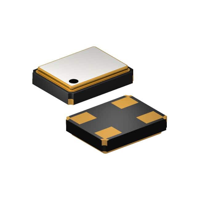
The SXT11412DA38-27.120MT is a compact, surface-mount crystal oscillator element designed for a nominal frequency of 27.120 MHz with a specified load capacitance of 12 pF. This frequency is commonly used in USB 3.0, wireless charging, and high-speed serial interfaces such as MIPI or LVDS where precise clocking is critical. The most fundamental circuit topology is the classic Pierce oscillator, where the crystal is connected between the oscillator amplifier’s input and output pins, with two load capacitors forming a capacitive divider to ground. For this crystal, each load capacitor should be selected such that the series combination of the two equals the specified 12 pF, plus any stray capacitance from the PCB traces and the microcontroller’s pin capacitance. As a practical starting point, use two 22 pF capacitors, then adjust downward to compensate for parasitic capacitance (typically 2–5 pF total). For a 27.120 MHz fundamental-mode crystal, avoid overtone operation by ensuring the oscillator’s gain is sufficient but not excessive; many modern MCUs have internal gain control, but if using a discrete inverter, add a series resistor (typically 100–470 Ω) in the feedback path to limit drive level and prevent over-driving the crystal.
When selecting supporting passives, prioritize capacitors with a tight tolerance (≤5%) and a stable temperature coefficient, such as C0G or NP0 dielectrics, to maintain frequency accuracy across the operating range. The load capacitors should be placed as close as possible to the crystal’s pins, with the ground side of each capacitor returning directly to the microcontroller’s ground pad through a dedicated via—do not share this via with other noisy digital returns. A parallel feedback resistor (1 MΩ to 10 MΩ) is often recommended to bias the inverter into its linear region; however, many integrated oscillators include this internally, so consult the MCU’s datasheet first. For the crystal itself, ensure that the ESR (equivalent series resistance) is within the oscillator’s negative-resistance budget; the SXT11412 series typically has an ESR of 60 Ω or less, which is suitable for most low-power CMOS oscillators. If a frequency-tuning varactor is needed for modulation or trimming, place it in series with one load capacitor, but be aware that this adds voltage-dependent capacitance and may degrade phase noise—use only when absolutely necessary.
PCB layout is paramount for reliable start-up and low jitter. Place the crystal and its load capacitors on the same layer as the microcontroller, ideally within a 5 mm radius of the oscillator pins. Keep the traces between the crystal and the MCU short (<10 mm) and equal in length to minimize differential phase error. Avoid routing any high-speed digital signals, especially clock or data lines, beneath or parallel to the crystal traces. A ground guard ring around the crystal region, connected to the main ground plane with multiple vias, provides shielding from adjacent switching noise. Do not route the crystal’s ground trace through a high-impedance path; instead, use a solid ground plane beneath the entire oscillator area. The crystal’s body should be placed with its longest dimension perpendicular to the PCB’s edge to reduce mechanical coupling to board flexure. For double-sided boards, avoid placing tall components or connectors that could induce mechanical stress on the SMD pads during handling or thermal cycling.
For EMC/EMI, the crystal’s fundamental frequency and its harmonics (54.24 MHz, 81.36 MHz, etc.) can radiate if the oscillator circuit is not properly decoupled. Add a 100 nF low-ESR ceramic capacitor directly at the VDD pin of the oscillator or MCU, plus a 10 µF bulk capacitor nearby. If the crystal traces are longer than 10 mm, consider using a series termination resistor (33–68 Ω) at the MCU output to reduce ringing and harmonic content—this also helps with radiated emissions. For stringent FCC or CISPR compliance, a ferrite bead placed in series with the crystal’s VDD supply can suppress common-mode noise coupling. Ensure that the crystal’s metal can (if present) is connected to ground—this provides a natural shield. In multi-layer PCBs, place the oscillator circuitry on an inner ground plane layer, but keep the crystal and capacitors on the outer layer to allow for rework. Avoid creating slot antennas by ensuring that the ground plane is continuous under the crystal and that no long, unbroken slots exist in the adjacent power or signal layers.
Common pitfalls include using load capacitors that are too large, which causes the oscillator to run below the nominal frequency, or too small, which raises the frequency and can push it out of spec. Another frequent error is assuming the crystal’s 12 pF load specifies the actual capacitor value—it is the total load seen by the crystal, so the two external capacitors must be roughly double that value in series. Over-driving the crystal due to excessive inverter gain can cause frequency drift and premature aging; check the drive level by measuring the voltage across the crystal with a high-impedance probe (1 MΩ, <2 pF) and ensure it is within the manufacturer’s maximum (typically 100 µW for this package). Also, beware of poor solder joints on the crystal’s pads—cold joints or excessive solder can introduce mechanical stress and cause frequency jumps. Finally, do not place the crystal near heat sources or in the path of cooling airflow, as frequency stability with temperature is already a challenge for 27.120 MHz parts.
During prototyping, start with a bare-bones circuit on a two-layer board using the recommended load caps and verify oscillation with an oscilloscope probe at the MCU’s clock output—not directly on the crystal pins, as the probe capacitance will detune the circuit. Use a 10× passive probe with a short ground spring to minimize added capacitance. Measure the frequency with a frequency counter or a spectrum analyzer; allow a 30-minute warm-up to observe thermal drift. Test start-up at the minimum supply voltage and lowest temperature specified for your design, as marginal conditions often expose weak oscillation. If using a microcontroller, read the actual clock frequency via an internal timer or PLL lock indicator to confirm the crystal is within ±30 ppm of 27.120 MHz. For final validation, perform a rapid thermal cycling test (−20°C to +70°C) while monitoring frequency stability; a shift of more than ±10 ppm beyond the crystal’s tolerance indicates a layout or component issue. Use a current probe on the VDD line to ensure the oscillator is not drawing excessive current, which suggests over-driving.