Crystal 11.0592MHz 17pF SMD: App Note & PCB Design Tips
The SXT32417DD07-11.0592MT is a fundamental-mode parallel-resonant crystal specified for an 11.0592 MHz frequency with a specified load capacitance of 17 pF. This value is critical: the oscillator circuit must present this exact capacitance to the crystal to pull the frequency to its nominal value. The most reliable topology is the classic Pierce oscillator, implemented using an integrated CMOS inverter (e.g., 74HCU04, 74LVC1GX04, or an MCU’s internal oscillator amplifier). Connect the crystal between the amplifier’s input and output pins, with two load capacitors—one from each crystal terminal to ground. For a parallel-resonant crystal, the total load capacitance seen by the crystal is the series combination of these two external capacitors plus the stray capacitance of the PCB traces and the IC’s pin capacitance. To achieve a nominal 17 pF load, choose each external capacitor to be approximately 30-33 pF if stray capacitance is about 3-5 pF, but always consult the MCU datasheet for its internal capacitance contribution. A 1 MΩ feedback resistor across the inverter input and output is essential to bias the inverter into its linear region; values from 1 MΩ to 10 MΩ work well, with 1 MΩ being typical for 11.0592 MHz. Additionally, a series damping resistor (typically 100 Ω to 1 kΩ) placed between the inverter output and the crystal can limit drive level and prevent over-driving, which is especially important for low-ESR crystals.
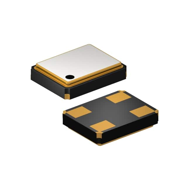
Component selection for the supporting passives is straightforward but demands attention to tolerance and temperature stability. Use C0G (NP0) ceramic capacitors for the load capacitors—these have a near-zero temperature coefficient, which will keep the oscillator frequency stable across temperature. Avoid X5R or Y5V dielectrics, as their capacitance can shift by 15-80% with voltage and temperature, causing frequency drift. The load capacitor values should be matched to within 1% to avoid frequency offset due to asymmetrical loading. The feedback resistor should be a thin-film resistor with a 1% tolerance; metal film is preferred over carbon for lower noise. The series damping resistor, if used, should be a standard 1% metal film type. For the crystal itself, the SXT32417DD07 is a 4-pad SMD package; ensure your footprint matches the pad dimensions provided by Suntsu’s datasheet. Always verify the crystal’s ESR (typically 40-60 Ω for this frequency) and drive level (usually 100 µW max) against the oscillator’s output current to prevent frequency aging or damage.
PCB layout is the most influential factor in oscillator performance. Place the crystal and its associated components as close as possible to the oscillator amplifier pins—ideally within 5 mm of trace length. Keep the traces from the crystal to the MCU short, direct, and of equal length to minimize parasitic inductance and capacitance asymmetry. Do not route any high-speed digital signals underneath or adjacent to the crystal traces. Surround the oscillator area with a ground pour on the top layer, and stitch it to the ground plane with multiple vias to create a low-impedance return path. Avoid placing vias under the crystal pads; instead, route the load capacitors’ ground connections directly to the nearest ground plane via. On multi-layer boards, place the crystal and its circuit on the same layer as the MCU to avoid plated through-holes in the signal path. If the crystal is on the bottom layer, ensure the top layer directly above is a solid ground plane, not a split or noisy power plane.
For EMC/EMI, the oscillator is a narrowband source at 11.0592 MHz, but harmonics can extend into the VHF/UHF range. The primary mitigation is to contain the RF energy within the local loop formed by the crystal, capacitors, and inverter. A low-ESR bypass capacitor (0.1 µF) placed directly at the oscillator’s power pins, with a ferrite bead in series with the supply, can isolate the oscillator from the rest of the board. Shield the oscillator area with a grounded metal can if the product must pass strict radiated emissions tests. Additionally, ensure the series damping resistor is large enough to limit the drive level—over-driving increases harmonic content. Keep the loop area of the ground return path minimized; a solid ground plane under the oscillator is mandatory. If the crystal is near a board edge, place a ground guard trace around it, but do not form a closed loop that could couple magnetic fields.
A common pitfall is misinterpreting the load capacitance specification. Using 17 pF capacitors directly on each pin is incorrect—that yields a total load of about 8.5 pF (series combination), pulling the frequency high by hundreds of ppm. Always calculate the required individual capacitor values as approximately twice the specified load, minus stray. Another frequent error is using an inverter with a very fast edge rate (e.g., standard 74HC) without a series resistor, leading to excessive drive and crystal damage. Always include the damping resistor. Also, some designers forget to check the MCU’s oscillator gain—if the internal amplifier is too weak, the crystal may not start reliably at low supply voltages; check the datasheet for the minimum transconductance. Finally, do not route the crystal traces near a switching regulator inductor or a high-current trace—magnetic coupling can cause frequency modulation.
For prototyping, solder the crystal and passives on a small adapter board with a ground plane, and keep leads short. First, verify the frequency with a frequency counter or an oscilloscope with a 10:1 probe connected to the oscillator output (not directly to the crystal, which would load it). Measure the exact frequency and compare to 11.0592 MHz; if it’s off by more than ±30 ppm, adjust the load capacitors. To tune, replace the fixed caps with a trimmer capacitor (e.g., 5-30 pF) on one side, but keep the other side fixed. Also, measure the drive level across the crystal using a current probe or by observing the output waveform—it should be sinusoidal, not clipped. For temperature testing, place the prototype in a thermal chamber and sweep from -40°C to +85°C, recording frequency drift. If the oscillator fails to start at low temperature, increase the feedback resistor or reduce the damping resistor. Finally, perform a startup test by toggling power and using a storage scope to capture the oscillation build-up—it should stabilize within 10 ms.