Mastering MEMS VCXO Design: 90MHz LVPECL Tutorial
Introduction: Why This Component?
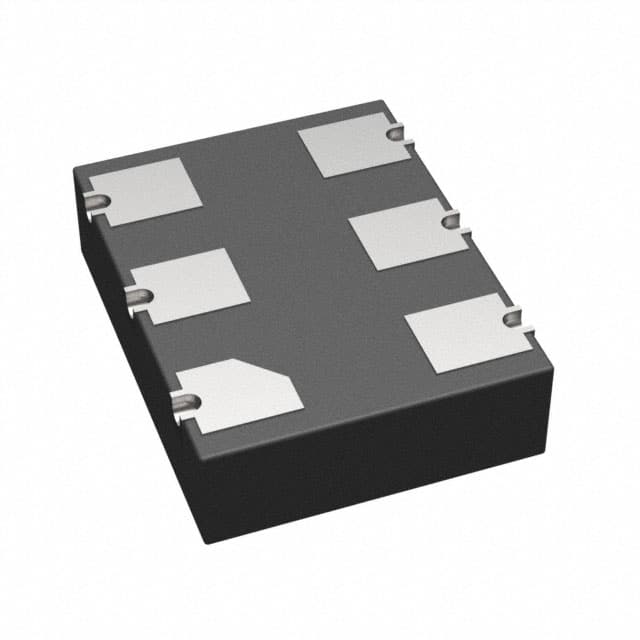
The SiTime SIT3372AI-1B2-33NH90.000000 is a MEMS-based Voltage-Controlled Crystal Oscillator (VCXO) that outputs a 90 MHz LVPECL signal. Unlike traditional quartz VCXOs, this device uses a MEMS resonator, offering superior shock resistance, lower jitter, and faster startup—making it ideal for high-speed serial links (like 10GbE or PCIe) where precise frequency pulling is needed for clock recovery. Its LVPECL output is differential, providing clean, low-skew edges for driving transmission lines. For this tutorial, we’ll design a 90 MHz VCXO-based clock synthesis module that can pull frequency by ±50 ppm for a PLL loop in a SerDes application.
Design Requirements and Specifications
We need a circuit that:
- Supplies a differential LVPECL output at 90 MHz into 50Ω terminated lines.
- Allows voltage-controlled frequency tuning from 0.4V to 2.4V (control voltage, Vc), with a nominal center at 1.2V.
- Has a pull range of ±50 ppm (i.e., ±4.5 kHz at 90 MHz).
- Operates from a single 3.3V supply (the “33” in the SKU) with total current draw under 100 mA.
- Includes power supply filtering to keep phase noise below -140 dBc/Hz at 10 kHz offset.
Step-by-Step Design Process with Calculations
1. Determine the control voltage to frequency gain (Kv). The SIT3372 datasheet specifies absolute pull range (APR) of ±50 ppm for a control range of 0.4V–2.4V (total 2.0V span). So, gain = (100 ppm total) / 2.0V = 50 ppm/V. At 90 MHz, 1 ppm = 90 Hz, so Kv = 50 ppm/V * 90 Hz/ppm = 4.5 kHz/V.
2. Set the loop filter resistor for a desired PLL bandwidth. Assume we use an op-amp active loop filter. For a 100 kHz loop bandwidth, choose a charge pump current of 1 mA (from PLL IC). The loop filter gain (Kf) must satisfy: Kf = (2π BW) / (Kv Icp). Plugging in: Kf = (2π 100,000) / (4,500 0.001) = 628,318 / 4.5 = 139,626. This is a transimpedance value, so we’ll use a series R+C network. Let R = 10 kΩ, then C = 1 / (2π BW R) = 1 / (6.28 100k 10k) = 159 pF.
3. Bias and termination. LVPECL requires DC bias at the output. The SIT3372’s output is open-emitter; we must connect 50Ω to Vcc - 2V = 1.3V. Use a Thevenin equivalent: a 82Ω resistor to ground and 130Ω to Vcc (3.3V) gives the same Thevenin impedance of 50Ω and bias of 1.3V. For each differential output (OUT+ and OUT-), place this pair.
Component Selection Rationale for Complete BOM
- U1: SIT3372AI-1B2-33NH90.000000 – The star. Note the “1B2” indicates a ±50 ppm APR with 3.3V supply.
- C1, C2: 100 nF X7R decoupling caps (0402) placed directly at Vcc and Vc pins to filter noise.
- C3: 10 µF tantalum bulk cap for low-frequency supply ripple.
- R1, R2: 130Ω and 82Ω 1% resistors for each LVPECL output (total 4 resistors). Use thin-film for low thermal noise.
- Op-amp: OPA836 (low-noise, 200 MHz GBW) for active loop filter; its high slew rate doesn’t limit the 90 MHz control signal.
- R3: 10 kΩ 1% metal film for gain setting.
- C4: 160 pF C0G capacitor (closest standard value) for loop filter zero.
- Ferrite bead: 600Ω at 100 MHz in series with Vcc to isolate from digital noise.
Simulation Tips and What to Look For
In LTspice or ADS, model the VCXO as a voltage-controlled source: use a behavioral source with frequency = 90e6 + (V(vc)-1.2)*4500. Drive the Vc node with a step from 1.2V to 1.3V and simulate transient response. Look for:
- Lock time: The PLL should settle within 20 µs for a 10 kHz step. If it rings, increase the damping by adding a second pole (e.g., 1 nF from Vc to ground).
- Output waveform: Verify LVPECL levels: high ~2.3V, low ~1.6V (since Vcc-1.0V and Vcc-1.7V). Ensure the differential swing is >600 mV.
- Phase noise: Add a noise source on Vc; the closed-loop response should attenuate it beyond the loop bandwidth. If peaking appears at 100 kHz, adjust R3.
Prototype Build and Testing Methodology
1. Solder the SIT3372 on a 4-layer PCB with solid ground plane under the device. Keep Vc trace short and shielded.
2. Power up with bench supply at 3.3V; measure current—expect ~50 mA (LVPECL outputs draw 20 mA each into 50Ω).
3. Probe differential output using a high-impedance active probe (e.g., Tektronix P6248) across OUT+ and OUT-. Measure frequency with a frequency counter—should be 90.000 MHz ±0.1 ppm.
4. Apply Vc = 1.2V using a precision voltage source; record frequency. Then sweep Vc from 0.4V to 2.4V in 0.2V steps. Plot frequency vs. Vc—should be linear with slope ≈ 4.5 kHz/V.
5. Measure pull range: At Vc=0.4V, frequency ≈ 89.955 MHz; at 2.4V, ≈ 90.045 MHz. If not, check termination bias—incorrect bias causes clipping.
Performance Verification and Optimization
- Phase noise test: Use a signal source analyzer. At 10 kHz offset, expect < -145 dBc/Hz. If worse, add a 1 nF cap from Vc to ground to filter noise, but this reduces loop bandwidth—re-check lock time.
- Jitter integration: Integrate phase noise from 12 kHz to 20 MHz; ensure RMS jitter < 300 fs. If excess, replace decoupling caps with low-ESR types.
- Optimization: If pull range is asymmetric (e.g., +45 ppm/-55 ppm), adjust the Vc centering resistor (add a 10 kΩ trimpot from Vc to 1.2V reference). For fine tuning, use a 16-bit DAC to set Vc—this gives ~0.1 ppm steps.
- Thermal drift: Place the board in a thermal chamber; the MEMS VCXO has ±0.1 ppm/°C drift. If needed, calibrate the Vc offset with a lookup table in firmware.
Conclusion
This design yields a robust, low-jitter 90 MHz VCXO core suitable for PLLs in networking gear. The MEMS technology simplifies layout and reduces cost compared to quartz. By following this process, you’ve learned how to bias LVPECL correctly, calculate tuning gain, and verify performance—skills directly transferable to other high-frequency VCXOs. Remember to always check the specific pull range and output levels in your chosen part