WE-MK SMT Inductor Application Guide: Optimize Circuit Design
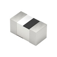
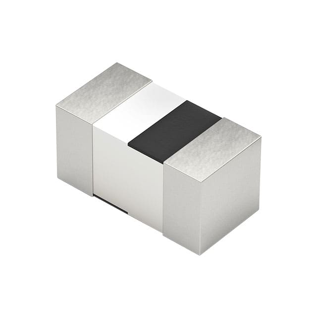
The WE-MK multilayer ceramic SMT inductor, specifically the 7447820043G, is a compact, high-frequency component designed primarily for signal conditioning and DC bias circuitry in RF and high-speed digital applications. Its monolithic ceramic structure provides a high self-resonant frequency (SRF) and tight inductance tolerance, making it ideal for impedance matching, resonant tank circuits, and decoupling networks where parasitic capacitance must be minimized. For optimal performance, integrate this inductor in series configurations for low-pass filtering or in shunt-to-ground arrangements for high-pass and band-stop filtering. Avoid using it in high-current power supply paths; its saturation current is limited, and its DC resistance (DCR) is non-negligible for power applications. Instead, pair it with a low-ESR ceramic capacitor in a classic LC pi-filter, positioning the inductor between two capacitors to achieve a balanced impedance match at the desired cutoff frequency. When designing a matching network for an antenna or a SAW filter, place the WE-MK inductor as close to the source or load as possible, using it as a series element to cancel out capacitive reactance, and always verify the component’s Q factor at the operating frequency—this part excels above 100 MHz, where its Q typically exceeds 50.
When selecting supporting passives, choose capacitors with NP0/C0G dielectric for temperature-stable resonant circuits, as X7R or Y5V types will introduce capacitance drift and distortion. For the shunt capacitors in a filter network, calculate the required value using the formula fc = 1/(2π√(LC)), but account for the inductor’s self-resonant frequency (SRF) which is typically around 2.5 GHz for this 43 nH part—operating above 20% of SRF will degrade the effective inductance. Use resistors with tight tolerance (1% or better) if you are building a bias tee, and ensure the DC blocking capacitor has a voltage rating at least twice the supply voltage to prevent dielectric breakdown. For impedance matching, use a vector network analyzer (VNA) to measure the inductor’s S-parameters, then select shunt capacitors that provide the conjugate match. Always check the inductor’s rated current (typically 300 mA for this series) and ensure your signal levels do not drive it into saturation; for RF bursts, derate to 70% of the rated current to avoid harmonic distortion.
PCB layout is critical for the WE-MK’s performance. Place the inductor on a solid ground plane with no ground cuts directly beneath it, as any slot in the return path will add parasitic inductance and shift the resonant frequency. Use microstrip or coplanar waveguide techniques for the traces leading to and from the component, keeping the trace width matched to a 50-ohm characteristic impedance. Route the inductor’s pads with short, direct connections—avoid long stubs or vias between the inductor and its associated capacitor, as each via introduces approximately 0.5 nH of parasitic inductance. For a differential pair, mirror the placement on both lines to ensure equal phase delay. Solder pad size should match the component’s 0603 footprint (1.6 x 0.8 mm) exactly; oversized pads will increase stray capacitance to ground. If you must route a signal under the inductor on an inner layer, ensure there is a ground plane between that signal and the inductor to prevent coupling. Keep the component at least 3 mm away from board edges and large metal shields to avoid eddy current losses.
For EMC/EMI mitigation, the WE-MK’s multilayer construction inherently provides low magnetic field leakage, but you can enhance its shielding by placing it in a shielded enclosure or by surrounding it with a ground stitch of vias—spaced at λ/20 of the highest operating frequency—to form a Faraday cage. When used in a filter, ensure the input and output traces are separated by a ground trace to prevent capacitive coupling that would bypass the filter’s attenuation. In mixed-signal designs, keep this inductor away from high-current switching nodes (e.g., DC-DC converter inductors) by at least 5 mm, or use a grounded copper pour between them. For conducted EMI, add a ferrite bead in series with the power line feeding the circuit, and place a 100 pF capacitor directly at the inductor’s supply pad to suppress high-frequency noise. If you observe spurious resonances, increase the series resistance slightly (e.g., 10 ohm in series with the inductor) to dampen the Q, but only if signal loss is acceptable.
A common pitfall is assuming this inductor behaves as an ideal component at high frequencies. Designers often forget that the SRF causes the impedance to become capacitive above resonance, leading to unexpected filter passbands. Always simulate the full network with S-parameter models from Würth Elektronik’s REDEXPERT tool or your own VNA measurements. Another frequent error is using the inductor for power supply decoupling where its low saturation current causes inductance collapse under DC bias, resulting in reduced filtering. Avoid placing the inductor in a feedback loop of an amplifier without checking its phase margin, as the added inductance can cause oscillation. Also, do not mix this ceramic inductor with ferrite-core inductors in the same matching network—their different temperature coefficients will shift performance. Finally, be wary of solder reflow profiles: excessive heat (above 260°C peak) can crack the ceramic body, so follow J-STD-020 reflow guidelines precisely.
For prototyping, build your circuit on an Rogers 4003 or FR4 board with a dedicated ground plane and use SMA connectors for measurement. Start with a bare-board calibration using a VNA to de-embed the test fixture’s parasitics. Solder the WE-MK using a hot-air rework station set to 240°C for no more than 30 seconds. Measure the insertion loss and return loss from 10 MHz to 3 GHz, and compare the results to your simulation. For a quick functional test, create a simple series resonator with a 1 pF capacitor and check the resonant dip on a spectrum analyzer using a tracking generator. If you see a >0.5 dB insertion loss anomaly, suspect a solder bridge or a cracked component—inspect under a microscope. For time-domain testing, apply a fast-edged square wave and use a high-impedance probe to check for ringing; any overshoot above 10% indicates impedance mismatch. Finally, stress-test the filter by sweeping the input power from -20 dBm to +10 dBm and monitoring the output for compression, which would reveal saturation effects.