TSC1031IDT Datasheet Guide: Current Sense IC 8SOIC Explained
The TSC1031IDT from STMicroelectronics is a high-side current sense amplifier delivered in an 8-pin SOIC package, and interpreting its datasheet correctly is essential for designing robust current monitoring into motor control, power management, and battery management systems. The device amplifies the small differential voltage developed across an external shunt resistor placed in the high side of a supply rail, translating it into a ground-referenced output proportional to load current. Understanding the datasheet begins with the electrical characteristics table, where parameters such as input offset voltage, gain, common-mode rejection ratio, and supply current define the real-world accuracy of the measurement. The input offset voltage is typically specified in the low microvolt range, and because this offset is amplified by the fixed gain, it directly sets the minimum resolvable current; designers should multiply the maximum offset by the gain to determine the worst-case output error floor. The gain is internally fixed and factory-trimmed, so the datasheet gives a gain error specification rather than a resistor tolerance, which simplifies the bill of materials but means the accuracy budget must account for gain drift over temperature.
Common-mode voltage range deserves particular scrutiny, because a high-side sense amplifier must survive and accurately measure signals far above its own supply. The TSC1031IDT is designed to operate with common-mode voltages well in excess of the supply rail, and the datasheet specifies both the operational range and the common-mode rejection ratio, typically expressed in dB across a defined frequency band. A high CMRR minimizes the error introduced when the supply rail moves, which is critical in motor drive circuits where the common-mode node swings rapidly. The supply voltage range and quiescent current complete the picture: the device operates from a low single supply, making it suitable for 3.3 V and 5 V systems, while the quiescent current specification informs the always-on power budget in battery-powered equipment.
Absolute maximum ratings define the boundaries beyond which the device may be permanently damaged, and they must never be treated as operating conditions. The maximum supply voltage, maximum common-mode input voltage, differential input voltage, and storage temperature are listed separately from the recommended operating conditions. The distinction matters because a designer may be tempted to run the part close to an absolute maximum during transient events; instead, the recommended operating conditions table should be used for continuous operation, and transient protection such as series resistors or clamp diodes should be added if the application exposes the inputs to inductive kickback or hot-swap spikes. Derating is primarily thermal: the datasheet provides a junction-to-ambient thermal resistance, and the maximum power dissipation must be reduced as ambient temperature rises. Electrostatic discharge ratings, usually given as human body model and charged device model figures, dictate the handling and board-level protection requirements.
A typical application circuit places a low-value shunt resistor between the supply and the load, with the two sense inputs connected across it through the recommended filter network. The datasheet's application information section usually shows a differential RC low-pass filter at the inputs to attenuate high-frequency noise and switching artifacts, with the capacitor value chosen to balance noise rejection against settling time. The reference pin allows the output to be offset, which is useful for bidirectional current sensing, and the datasheet explains how to drive it from a divider or a dedicated reference. The output is typically connected to an ADC input, and the output voltage swing specifications define how close to the rails the amplifier can drive, which determines the usable dynamic range of the measurement.
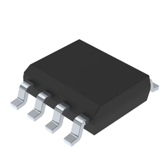
The 8-pin SOIC pinout is standardized, and the datasheet's pin configuration diagram identifies the supply, ground, sense inputs, reference, and output pins. Package considerations include the thermal pad if present, the lead finish for solderability, and the moisture sensitivity level for reflow assembly. The SOIC body is compact enough for dense layouts but still hand-solderable, and the pin spacing supports standard PCB design rules. Creepage and clearance should be verified when the common-mode voltage is high, since the package pins may be close together relative to the applied potential.
Thermal management focuses on keeping the junction temperature below the specified maximum. Because the TSC1031IDT dissipates little power internally, the dominant thermal path is through the package leads to the copper traces. The datasheet's thermal resistance values, combined with the calculated internal dissipation from supply voltage and quiescent current, allow a straightforward junction temperature estimate. Layout guidance typically recommends a ground plane and short, wide traces at the supply and output pins to spread heat and reduce parasitic inductance.
Finally, the characteristic curves and timing diagrams translate static specifications into dynamic behavior. Gain versus frequency plots reveal the amplifier's bandwidth and phase margin, showing where the response rolls off and whether peaking occurs. CMRR and PSRR versus frequency curves indicate how rejection degrades at higher frequencies, which matters when the load switches at tens of kilohertz. Step response and settling time diagrams define how quickly the output reaches a valid reading after a current transient, a key parameter for overcurrent protection loops. Output voltage versus common-mode voltage curves expose nonlinearity near the extremes of the input range. Reading these curves alongside the tabulated limits gives the engineer a complete picture of performance, enabling an informed selection of the TSC1031IDT for a given accuracy, bandwidth, and thermal budget.