Designing with LTC1293DCSW: 12-Bit ADC/DAS Tutorial
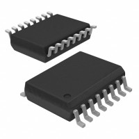
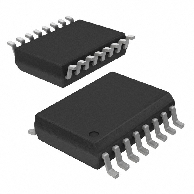
The LTC1293DCSW#PBF from Analog Devices is a 12-bit successive-approximation ADC with a maximum throughput of 46.5 kSPS, packaged in a 16-pin SOIC. What makes it ideal for a hands-on tutorial is its integrated 8-channel multiplexer, differential input capability, and on-chip sample-and-hold—all in a single IC. Unlike many modern ADCs that require external drivers and reference buffers, this part accepts analog inputs directly and communicates over a simple 3-wire SPI-compatible serial interface. That combination means you can build a complete data acquisition system with just a handful of passives, making it perfect for learning the full signal chain from sensor to digital output.
For this tutorial, we will design a 4-channel temperature and pressure monitoring node. The design requirements are: measure four single-ended analog signals (0–4.096 V), sample each channel at 1 kSPS, achieve 12-bit resolution with less than ±2 LSB total unadjusted error, and interface to a 3.3 V microcontroller. The LTC1293 runs from a single 5 V supply but its digital I/O is compatible with 3.3 V logic when the supply is properly sequenced. We will use the internal reference? No—the LTC1293 requires an external reference. We will select a 4.096 V reference to match our full-scale input, giving an LSB size of 1 mV.
Step 1: Reference and supply. The ADC’s reference input (VREF) sets the full-scale range. For 0–4.096 V inputs, use a precision 4.096 V reference such as the ADR4540 (0.1% initial accuracy, 5 ppm/°C). Decouple VREF to analog ground with a 1 µF ceramic capacitor in parallel with 0.1 µF. The analog supply (VDD) should be 5 V ±5%, and the digital supply (VCC) can be 3.3 V. Place a 10 µF tantalum and 0.1 µF ceramic at each supply pin.
Step 2: Analog input conditioning. The LTC1293’s input range is 0 V to VREF. For a typical 4–20 mA pressure transmitter, use a 200 Ω precision resistor (0.1%, 25 ppm/°C) to convert current to voltage: 4 mA → 0.8 V, 20 mA → 4.0 V. This leaves headroom below 4.096 V. For temperature sensors like a 10 kΩ thermistor, use a voltage divider with a 10 kΩ 0.1% resistor to VREF. Add a 1 kΩ series resistor and 100 nF capacitor to each analog input to form a low-pass filter with a cutoff of 1.6 kHz—this reduces noise without slowing the 1 kSPS sampling.
Step 3: Digital interface and timing. The LTC1293 uses a 3-wire interface: CS, SCLK, and DOUT. Connect CS to a GPIO, SCLK to the SPI clock (max 1 MHz), and DOUT to MISO. The conversion is initiated by a start bit followed by a 3-bit channel address. After 12 clock cycles, the 12-bit result is shifted out MSB-first. At 1 kSPS, you have 1 ms per sample—plenty of time for a 16-bit SPI transfer at 1 MHz. Use a series 33 Ω resistor on SCLK to reduce ringing.
Step 4: Component selection rationale. The BOM includes: LTC1293DCSW#PBF (ADC), ADR4540 (reference), 200 Ω 0.1% (current-to-voltage), 10 kΩ 0.1% (thermistor divider), 1 kΩ 1% (input filter), 100 nF C0G (filter), 1 µF X7R (reference decoupling), 10 µF tantalum (supply bulk), and 0.1 µF ceramic (supply bypass). All passives are 0805 size for easy hand soldering. The ADR4540 was chosen over a shunt reference because it sources up to 10 mA, which the ADC’s reference input does not require, but it provides excellent line and load regulation.
Simulation tips: In LTspice, model the ADC as an ideal 12-bit quantizer with a 4.096 V reference and a 1 kSPS sample clock. Add a 1 kΩ/100 nF RC filter at each input and inject a 10 mVPP 60 Hz noise source to see the filter’s effect. Look for code transitions—the output should change by exactly 1 LSB (1 mV) per 1 mV input change. Check that the digital output settles within 1 µs after the 12th clock edge. Also simulate the reference’s transient response when the ADC samples—a 1 µF capacitor should keep droop below 0.5 LSB.
Prototype build and testing: Assemble on a ground-plane PCB or a solderless breadboard with short leads. First, verify the reference voltage with a 6.5-digit DMM—it must be 4.096 V ±2 mV. Next, apply a known DC input (e.g., 2.048 V from a calibrated source) and read the digital output. The expected code is 2048. Test all four channels by switching the multiplexer address. Use a function generator to apply a 10 Hz sine wave and capture 1000 samples—plot the FFT to check for missing codes and harmonic distortion.
Performance verification and optimization: Calculate INL and DNL by sweeping the input from 0.1 V to 4.0 V in 1 mV steps using a precision voltage source. The LTC1293 guarantees ±1 LSB INL and ±1 LSB DNL. If you see larger errors, check the reference stability and analog ground integrity. To reduce noise, average 4 samples in firmware—this improves effective resolution to 13 bits at the cost of throughput. For best results, keep the analog ground separate from digital ground and tie them at a single point under the ADC. With these steps, your 12-bit DAS will reliably digitize sensor signals with less than 0.1% error.