Design Guide for 10-Position 1.27mm SMD Headers (5-147382-1)
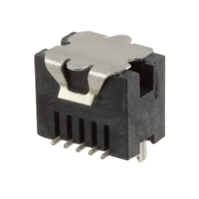
The TE Connectivity AMP Connectors 5-147382-1 is a 10-position surface-mount header with a 1.27 mm (0.05 in) pitch. This fine-pitch connector is designed for board-to-board or board-to-cable applications where space is at a premium. It features a shrouded, polarized housing that prevents mis-mating, and its SMD termination makes it ideal for automated reflow assembly. For this tutorial, we will design a compact sensor breakout board that uses this header to interface a microcontroller with a remote sensor module. The 1.27 mm pitch keeps the PCB footprint small while still allowing hand soldering with proper technique, making it a great choice for prototyping and low-volume production.
Design Requirements and Specifications
We need a 10-pin interface carrying power, ground, and eight signal lines for a digital sensor array. The system operates at 3.3 V with a maximum current of 500 mA per power pin. Signal speeds are modest (up to 10 MHz SPI), so signal integrity is manageable but not trivial. The connector must survive reflow soldering at 260 °C peak and operate from -40 °C to +85 °C. The board will be a two-layer FR-4, 1.6 mm thick, with 1 oz copper. We also require reverse-polarity protection and ESD suppression on the signal lines.
Step-by-Step Design Process
First, calculate the trace width for 500 mA on 1 oz copper with a 10 °C temperature rise. Using the IPC-2221 formula, a 0.25 mm (10 mil) trace is sufficient, but we will use 0.4 mm (16 mil) for margin and lower inductance. Next, determine the pad geometry. The 5-147382-1 has a lead pitch of 1.27 mm and a pad width of approximately 0.6 mm. We set the PCB pad length to 1.6 mm and width to 0.7 mm to allow a small fillet. The solder mask opening should be 0.1 mm larger than the pad on all sides.
For the power pins (pins 1 and 2 for 3.3 V, pins 9 and 10 for GND), we double the number of pins to reduce contact resistance and current density. Place a 100 nF decoupling capacitor within 2 mm of pin 1. Add a 10 µF bulk capacitor near the connector. For ESD protection, use a TVS diode array (e.g., SMF05C) on the four highest-speed signal lines (pins 3–6).
Impedance control is not critical at 10 MHz, but keep signal traces short and avoid stubs. Route the clock line (pin 3) with a ground guard trace on both sides. Use a solid ground plane on layer 2. The connector’s 1.27 mm pitch means we can route two traces between adjacent pads if we use 0.15 mm traces and 0.15 mm spacing, but we will keep one trace per gap for simplicity and reliability.
Component Selection Rationale
The 5-147382-1 is chosen for its 1.27 mm pitch, which balances density and manufacturability. Its SMD design eliminates through-hole drilling, reducing board cost. The shrouded housing prevents accidental disconnection. For the mating half, use a compatible 10-position IDC ribbon cable connector (e.g., TE 1-215911-0). The TVS array (SMF05C) offers low capacitance (<5 pF) and fast response. The decoupling capacitors are X7R ceramic for stability. The bulk capacitor is a 10 µF tantalum or ceramic. All components are rated for the industrial temperature range.
Simulation Tips
Before layout, simulate the power delivery network in SPICE. Model the connector as a series resistance of 20 mΩ per pin and an inductance of 2 nH per pin. Add the decoupling capacitors and a current step load of 500 mA with a 1 µs rise time. Check that the voltage droop at the sensor supply pin stays below 100 mV. For signal integrity, run a simple IBIS simulation on the SPI clock line. Look for overshoot and ringing. If overshoot exceeds 0.5 V, add a 22 Ω series resistor at the source. Also simulate the ESD clamp response using a human body model (8 kV, 150 pF, 330 Ω). Verify that the clamp voltage stays below the sensor’s absolute maximum rating.
Prototype Build and Testing
Order the PCB with a solder paste stencil. Apply lead-free paste (SAC305) and place the connector using a fine-tip tweezer. Reflow with a profile peaking at 245 °C for 30 seconds. Inspect the joints under a microscope for bridging and insufficient solder. Use a multimeter to check continuity between the header pins and the corresponding test points. Power the board with a current-limited supply set to 3.3 V and 200 mA. Measure the voltage at the sensor connector with a scope. Then connect the sensor module and run a loopback test: send a known pattern over SPI and verify the received data. For mechanical testing, mate and unmate the connector 20 times, then recheck continuity.
Performance Verification and Optimization
Measure the insertion loss of the power path by injecting a 1 kHz square wave and observing the rise time. With 20 mΩ and 2 nH per pin, the expected rise time is under 10 ns. If you see excessive ringing, add a small RC snubber. For thermal verification, run 500 mA through the power pins for 10 minutes and measure the connector body temperature with an IR thermometer. The temperature should rise less than 15 °C above ambient. If it exceeds this, add more copper area around the pads or use two pins per power net. Finally, perform a 100-cycle mating test and monitor contact resistance; it should remain below 30 mΩ. Optimize by choosing a gold-plated version of the header if the environment is humid or corrosive.