Application Note: CN100A110-15 15V 100W DC-DC Converter Design
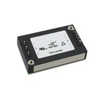
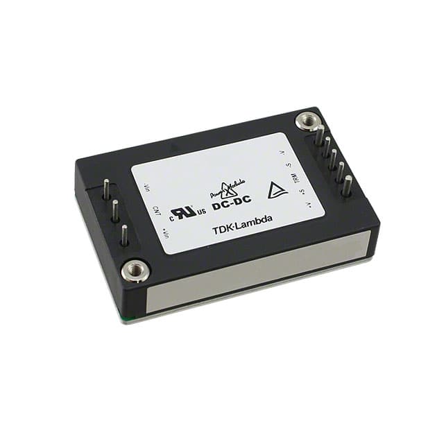
The TDK-Lambda CN100A110-15 is a 100 W, 15 V output isolated DC-DC converter designed for nominal 110 VDC input rails such as those found in railway, industrial, and telecom equipment. It delivers up to 6.7 A at 15 V with typical efficiency in the high 80s to low 90s percent range, and it comes in an industry-standard half-brick footprint with through-hole pins. Because the input is a high-voltage DC rail rather than a low-voltage bus, the design practices that surround this converter differ from those for a typical 24 V or 48 V input module. The notes below focus on the practical decisions that determine whether a design passes EMC, survives transients, and runs cool.
Recommended circuit topologies and design best practices. This converter is a fixed-ratio, isolated switching regulator, so it should be treated as a complete power stage rather than as a controller you wrap with external magnetics. The most common topology for a 110 V input, single 15 V output application is a simple point-of-load arrangement: a front-end input filter, the module, and an output filter feeding the load. If you need multiple rails, do not parallel the outputs of two CN100A110-15 units directly, because their internal references and switching phases are not synchronized; instead, derive secondary rails from the 15 V output with a downstream non-isolated buck or LDO, or use a separate converter with an appropriate input range. For higher current, use a single module and distribute the 15 V, keeping trace and cable drops in mind. Always respect the module's minimum load requirement if one is specified in the datasheet, and never operate it with the output open while the input is live unless the datasheet explicitly permits it. Inrush control on the 110 V input is important: a pre-charge resistor bypassed by a relay or a suitable NTC thermistor limits the surge into the input capacitor bank and protects upstream fuses and contactors.
Component selection guidelines for supporting passives. The input capacitor is the single most important external component. Choose a low-ESR electrolytic or polymer capacitor rated for at least 200 VDC with ripple current capability well above the module's input ripple, and place a 1 uF to 10 uF ceramic or film capacitor in parallel close to the input pins for high-frequency decoupling. Keep the input capacitor within a few centimeters of the module; long input leads add inductance that can cause instability and ringing. On the output, use low-ESR capacitors rated for the full 15 V plus margin, again with a ceramic bypass near the load. The output filter capacitor value should follow the datasheet's recommended range, since too little capacitance causes excessive ripple and too much can affect the loop response of some modules. For the sense and trim pins, use short, direct connections; if you use the trim function, a small multi-turn potentiometer or fixed resistor divider with 1 percent tolerance is appropriate. Fusing should be selected for the maximum input current at minimum input voltage plus margin, and a TVS or metal-oxide varistor across the input protects against inductive kickback from the 110 V rail.
PCB layout recommendations and routing tips. Treat the input loop as a tight, low-inductance circuit: place the input capacitor, the fuse, and the module's input pins as close together as possible, and route the return path directly under the positive trace on an adjacent layer to minimize loop area. Use wide copper pours for both input and output power paths; a 100 W converter at 15 V carries significant current, so size traces for the expected current with a comfortable margin and consider using multiple vias in parallel where you transition layers. Keep the output return separate from the input return and join them at a single point near the module to avoid ground loops. Route the trim and enable pins away from switching nodes and clock lines, and keep any sensitive analog or feedback traces at least a few millimeters from the module's switching area. Place the module so that its thermal pad or baseplate has a clear path to the enclosure or a heatsink, and provide thermal vias under any pad that needs to conduct heat into the board.
EMC/EMI considerations and mitigation strategies. A 110 V input, 100 W converter will generate both differential-mode and common-mode noise, and meeting EN 55011 or EN 55022 limits usually requires an input filter beyond the module's internal components. Start with a two-stage differential filter: a common-mode choke followed by X capacitors across the input and Y capacitors from each input line to chassis ground. Keep the Y capacitor values small enough to satisfy leakage current limits for your safety class, and place the filter as close to the module input as possible. Shield the input and output wiring, and if the module is mounted on a metal chassis, bond the chassis to the board ground at multiple points. Snubbers across any external switching devices, if used, should be tuned on the bench rather than guessed. Radiated emissions often come from long input or output cables acting as antennas, so ferrite sleeves on those cables are a practical last-resort fix.
Common design pitfalls and how to avoid them. The most frequent failure is undersized or poorly placed input capacitance, which causes input voltage sag, instability, and audible noise. Another is ignoring the minimum input voltage under load: the CN100A110-15 expects a nominal 110 V rail, and if your source droops during transients, the module may shut down or hiccup. Do not assume the module's isolation barrier tolerates unlimited common-mode voltage; respect the isolation rating and keep the secondary referenced to a well-defined ground. Avoid long, unshielded sense lines and do not connect the trim pin to anything other than a proper resistor network. Finally, do not ignore thermal derating: at 100 W output, even 90 percent efficiency means 11 W of heat, and without adequate airflow or heatsinking the module will enter thermal shutdown.
Prototyping tips and bench testing procedures. Build the first article on a board that mirrors the final layout as closely as possible, including the input filter and grounding scheme, because a breadboard will not predict EMC or thermal behavior. Before applying full input voltage, verify with a current-limited bench supply set to 110 V and a low current limit, and check that the output rises cleanly and stays in regulation. Measure input and output ripple with a proper differential probe or a short-ground-lead technique, not a long ground clip. Load the output with an electronic load and sweep from no load to full load while monitoring module temperature with a thermocouple on the baseplate. Run a thermal soak at full load for at least 30 minutes. For EMC, pre-scan with a near-field probe before formal testing to locate hot spots, and test at both minimum and maximum input voltage. Finally, cycle the input power repeatedly to verify inrush behavior and check that no component is stressed beyond its ratings.