BCX54-16,115 Datasheet Guide: NPN 45V 1A SOT89 Transistor Explained
The Nexperia BCX54-16,115 is a medium-power NPN bipolar junction transistor housed in the compact SOT89 surface-mount package. Understanding its datasheet requires familiarity with the interplay between electrical specifications, thermal constraints, and the practical demands of real-world circuits. This guide walks through the essential parameters an engineer must evaluate before committing the device to a design.
The headline specifications indicate a collector-emitter voltage (VCEO) of 45 V, a continuous collector current (IC) of 1 A, and a DC current gain (hFE) grouped as the "16" suffix, which corresponds to a gain range of 100 to 250 at IC = 150 mA. In practice, the 45 V rating defines the maximum steady-state voltage the device can withstand across its collector and emitter terminals with the base open. Designers should treat this as a hard ceiling and apply margin, particularly in inductive load switching where voltage spikes can momentarily exceed the supply rail. The 1 A current rating is not unconditional; it depends on the mounting conditions and ambient temperature, a point elaborated in the thermal section below. The hFE grouping matters because it determines base drive requirements. With a minimum gain of 100, a base current of 10 mA ensures saturation at 1 A, assuming the device is overdriven sufficiently to minimize VCE(sat).
Absolute maximum ratings form the boundary beyond which reliable operation cannot be guaranteed. For the BCX54-16,115, the collector-emitter voltage is 45 V, the collector-base voltage (VCBO) is 45 V, and the emitter-base voltage (VEBO) is typically 5 V. The low emitter-base rating is often overlooked; reverse biasing the base-emitter junction beyond 5 V can degrade gain or destroy the device. Collector current is rated at 1 A continuous and 2 A peak, while total power dissipation (Ptot) is 1.3 W at an ambient temperature (Tamb) of 25 °C when mounted on a ceramic substrate. Derating is mandatory: above 25 °C, the permissible power decreases linearly at approximately 10.4 mW/°C. At 100 °C ambient, for instance, the device can safely dissipate only about 520 mW. Junction temperature (Tj) must never exceed 150 °C, and storage temperature ranges from -65 °C to +150 °C. These derating curves are not suggestions; ignoring them leads to thermal runaway and premature failure.
A typical application circuit for the BCX54-16,115 is a low-side switch driving a relay, solenoid, or LED string from a logic-level signal. The emitter connects to ground, the collector to the load, and the load's other terminal to a positive supply. A base resistor limits current from the driving source, and a pull-down resistor from base to emitter ensures the transistor remains off when the driver is high-impedance. For inductive loads, a flyback diode across the load clamps the voltage spike when the transistor turns off. The base resistor value is calculated from the desired collector current, the minimum hFE, and the driver voltage. For 500 mA with hFE = 100, base current must be at least 5 mA; a 1 kΩ resistor from a 5 V logic output provides roughly 4.3 mA, which is marginal. Using a 680 Ω resistor yields about 6.3 mA, ensuring hard saturation and minimizing VCE(sat), typically 0.5 V at 500 mA. Lower VCE(sat) reduces power dissipation, which directly eases thermal constraints.
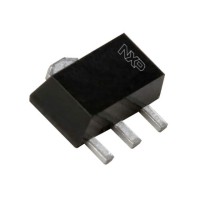
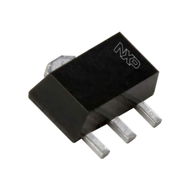
The SOT89 package is a three-lead plastic surface-mount outline with a collector tab that also serves as a thermal pad. Pin 1 is the base, pin 2 is the collector, and pin 3 is the emitter, but the collector is also connected to the exposed tab on the bottom of the package. This tab must be soldered to a copper pad on the PCB for both electrical connection and heat dissipation. The footprint requires careful layout: a generous copper area under the tab acts as a heatsink, and thermal vias to an inner or backside copper plane further reduce thermal resistance. The junction-to-ambient thermal resistance (Rth(j-a)) is approximately 95 K/W on a standard footprint, but can drop to 60 K/W or lower with enhanced copper. This parameter is the single most important number for determining safe operating current at elevated ambient temperatures.
Thermal management begins with calculating junction temperature using Tj = Tamb + (Pdiss × Rth(j-a)). Power dissipation is the sum of collector dissipation (VCE × IC) and base dissipation (VBE × IB), though the latter is usually negligible. If the calculated Tj exceeds 125 °C, the designer must either reduce current, lower the duty cycle, improve the thermal path, or select a larger package. Pulsed operation allows higher peak currents because the thermal time constant of the die is much shorter than the pulse duration, but the average power must still respect the derating curve. For continuous 1 A operation, VCE(sat) of 0.5 V yields 500 mW dissipation. With Rth(j-a) = 60 K/W, the junction rises 30 °C above ambient. At 85 °C ambient, Tj reaches 115 °C, which is acceptable but leaves little margin. At 100 °C ambient, Tj reaches 130 °C, dangerously close to the 150 °C limit.
Interpreting the characteristic curves is essential for predicting real behavior. The DC current gain versus collector current curve shows hFE peaking around 100–200 mA and falling at both low and high currents. At 1 A, hFE may drop to 40 or lower, meaning base drive must increase accordingly. The collector-emitter saturation voltage versus collector current curve reveals that VCE(sat) rises sharply above 500 mA, increasing dissipation. The safe operating area (SOA) graph plots collector current against collector-emitter voltage, with boundary lines for DC, 1 ms, and 10 µs pulses. The DC line slopes downward at higher voltages due to second breakdown, so operating at 45 V and 1 A simultaneously is forbidden. The thermal derating curve is a straight line from 1.3 W at 25 °C to zero at 150 °C. Finally, the switching time curves show turn-on and turn-off times in the tens of nanoseconds, making the device suitable for moderate-frequency switching up to a few hundred kilohertz. Always cross-reference these curves with the actual operating conditions; a datasheet curve taken at 25 °C may shift significantly at 100 °C, particularly for gain and saturation voltage.