MEMS OSC XO 32.7680MHz Datasheet Guide: SIT1602BI-32 Explained
The SiTime SIT1602BI-32-XXS-32.768000 is a MEMS-based oscillator delivering a fixed 32.7680 MHz output with high/low CMOS compatibility. Unlike legacy quartz crystal oscillators, this device integrates a silicon MEMS resonator with a programmable analog front-end, yielding exceptional stability and immunity to environmental stressors. When interpreting its datasheet, the first electrical parameters to internalize are the supply voltage range, output logic levels, and current consumption. The part number suffix "XXS" indicates a specific supply voltage option—typically 1.8 V, 2.5 V, or 3.3 V—so the engineer must confirm the exact variant before designing the power rail. The output is H/LV-CMOS, meaning it swings between a high level near Vdd and a low level near ground, with defined VOH and VOL thresholds. In practice, this means the oscillator can directly drive standard CMOS inputs without level shifting, provided the receiver’s input threshold aligns with the chosen Vdd. The 32.7680 MHz frequency is not a real-time clock frequency; it is a high-speed clock for serializers, FPGAs, or networking PHYs. The datasheet’s frequency stability specification, often ±20 ppm or ±25 ppm over temperature, dictates the maximum allowable deviation for asynchronous protocols like UART or USB. A tighter stability grade (e.g., ±10 ppm) costs more but reduces bit errors in high-temperature environments.
Absolute maximum ratings define the stress limits beyond which the device may suffer permanent damage. For this SiTime MEMS oscillator, typical abs-max values include a supply voltage of –0.3 V to +4.0 V, input voltage on any pin of –0.3 V to Vdd+0.3 V, and storage temperature from –65°C to +150°C. These are not operating conditions. Derating is critical: never operate at the absolute maximum supply voltage, even briefly, because internal ESD diodes or charge pumps can latch up. Instead, design the power supply to stay within the recommended operating range, usually ±10% of nominal Vdd. For example, a 3.3 V variant should be powered from a 3.0 V to 3.6 V rail. Also derate the output current: the datasheet’s test condition for VOH/VOL typically assumes a load of 15 pF or 10 kΩ to Vdd/2. If your load capacitance exceeds 30 pF, the rise/fall times will degrade, and the effective output swing may shrink. Always subtract margin from the maximum operating junction temperature (often 125°C) when the ambient exceeds 85°C, because self-heating from the oscillator’s own power dissipation adds a few degrees.
The typical application circuit for the SIT1602BI-32-XXS-32.768000 is deceptively simple, but layout and decoupling determine real-world performance. Connect Vdd to the positive supply through a low-ESR ceramic capacitor of 0.1 µF placed within 2 mm of the Vdd pin, and add a 1 µF bulk capacitor nearby. The ground pin must return to a clean analog ground plane, not a noisy digital ground. The output pin drives the clock input of the target IC; if the trace length exceeds 5 cm, add a series termination resistor of 22 Ω to 33 Ω at the source to damp reflections. Do not add a pull-up or pull-down on the output unless the datasheet explicitly permits open-drain mode—this device is push-pull CMOS. The OE (output enable) pin, if present, should be tied to Vdd for always-on operation or driven by a logic signal with rise/fall times under 100 ns. A common mistake is to leave OE floating; internal pull-ups may or may not exist, so consult the pin description table. For low-power applications, the standby current when OE is low is typically under 50 µA, but the startup time from disable to stable output can be 5–10 ms, which matters for power-sequenced systems.
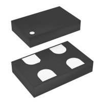
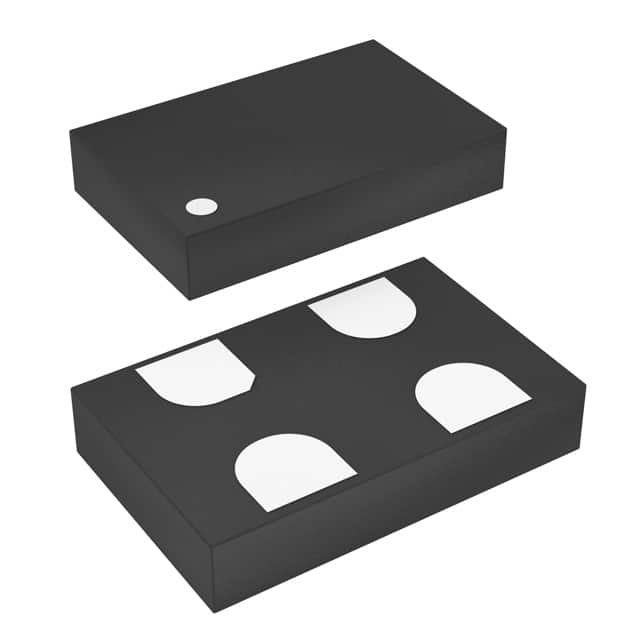
Pin configuration follows a standard 4-pin or 6-pin package, often a 3.2 x 2.5 mm or 2.5 x 2.0 mm ceramic package. The SKU "SIT1602BI-32-XXS-32.768000" implies a 4-pin package: Pin 1 is OE or NC (no connect), Pin 2 is GND, Pin 3 is Output, and Pin 4 is Vdd. Always verify against the specific package drawing, because some variants swap OE and GND. The package is hermetic and RoHS-compliant, but the solder pad geometry must match the recommended land pattern to avoid tombstoning during reflow. Because MEMS oscillators are less sensitive to board flex than quartz, they tolerate standard FR-4 mounting without special cutouts. However, the package’s thermal pad, if present, should be soldered to a ground plane for heat spreading—not for electrical ground, as the pad may be internally connected to GND or floating.
Thermal management for this device is straightforward but non-negligible. The maximum operating junction temperature is typically 125°C, and the thermal resistance from junction to ambient (θJA) is around 150°C/W for a 4-pin package on a JEDEC board. At 3.3 V and 10 mA typical current, power dissipation is 33 mW, causing a junction rise of about 5°C above ambient. That is safe up to 85°C ambient, but at 105°C ambient, the junction reaches 110°C—still within limits but with reduced lifetime. The datasheet’s frequency stability versus temperature curve shows a parabolic or piecewise-linear shift; MEMS resonators are compensated, so the shift is often less than ±10 ppm from –40°C to +85°C. For higher temperatures, derate the supply voltage slightly or add airflow. Never rely on the package alone to dissipate heat; use a ground plane with thermal vias if the oscillator sits near a power amplifier or FPGA.
Timing diagrams and characteristic curves reveal dynamic behavior that static tables cannot. The datasheet will show a waveform with rise time (tr) and fall time (tf) typically 2–5 ns for a 15 pF load, measured from 10% to 90% of Vdd. Duty cycle is specified as 45% to 55%, which is critical for double-data-rate interfaces. The startup waveform shows a delay from power-on to first valid clock edge—often 5 ms—followed by a stable period. Jitter curves plot phase noise versus offset frequency; for this MEMS oscillator, integrated jitter from 12 kHz to 20 MHz is typically 1–2 ps RMS. That low jitter makes it suitable for SerDes reference clocks. The frequency versus supply voltage curve is nearly flat (less than ±1 ppm/V), but the frequency versus load capacitance curve slopes downward—adding 10 pF of stray capacitance can pull the frequency by 5–10 ppm. Always measure your board’s actual load and compare to the datasheet’s test condition. Finally, the enable/disable timing diagram shows that when OE goes low, the output enters a high-impedance state within 100 ns, but the internal oscillator may take milliseconds to restart. For glitch-free clock switching, use a dedicated clock mux rather than toggling OE.