MEMS VCXO 133.6500MHz HCSL Application Note: Design Guide for SIT3372AI
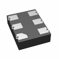
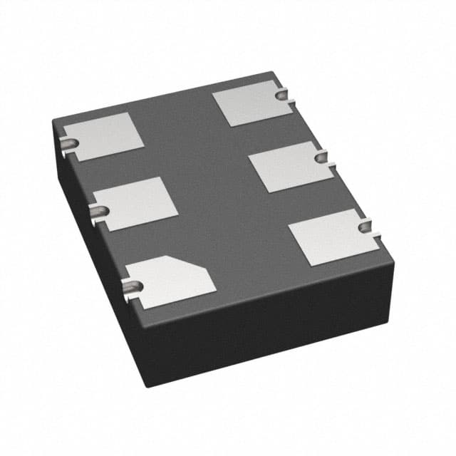
The SiTime SIT3372AI-4B9-33NH133.650000 is a differential MEMS VCXO that delivers a 133.6500 MHz output with HCSL signaling from a 3.3 V supply. Its architecture combines a silicon MEMS resonator with a programmable analog phase-locked loop, offering excellent jitter performance, tight temperature stability, and a wide pull range for clock recovery and jitter attenuation applications. The device is particularly well suited for 100G/400G optical transport, synchronous Ethernet, and high-speed SerDes reference clocking where low phase noise and precise frequency control are critical. Because the output is HCSL, the VCXO expects to drive 50 Ω transmission lines to ground, and the design must respect the DC and AC characteristics of that interface. This application note covers practical steps to integrate the device reliably from schematic capture through bench validation.
For most applications, the recommended topology is a simple point-to-point connection from the VCXO output to the receiving device, with each of the differential outputs (OUT+ and OUT−) terminated to ground through a 50 Ω resistor placed as close as possible to the receiver input. HCSL outputs are current-mode, so the termination resistors provide the return path and set the output swing. Do not add AC coupling capacitors unless the receiver requires them; if AC coupling is necessary, place the capacitors after the termination resistors so the DC bias of the HCSL output is preserved. The voltage control pin (VC) should be driven from a low-noise DAC or filtered PWM source, and a series resistor of 10 kΩ to 50 kΩ in combination with a 0.1 µF capacitor to ground forms a simple low-pass filter that reduces control-line noise without compromising loop bandwidth. Keep the VC trace short and guard it from digital noise.
Supporting passives are straightforward but require attention to tolerance and temperature coefficient. Use 1% or better thin-film resistors for the 50 Ω terminations; standard thick-film parts can drift enough to degrade output swing and eye quality. Place a 0.1 µF X7R or C0G decoupling capacitor directly between each VDD pin and the ground plane, and add a 1 µF bulk capacitor nearby. For the VCXO control input, a C0G capacitor in the filter network prevents piezoelectric noise. If the design uses a ferrite bead for supply isolation, choose one with a high impedance in the 100 MHz to 1 GHz range, but verify that its DC resistance does not drop the supply below the 3.3 V ±5% operating window. Avoid using a single decoupling capacitor for multiple supply pins; each pin should have its own high-frequency bypass.
PCB layout is critical because the HCSL outputs are fast edges that can couple into nearby traces. Route the differential pair as a 100 Ω differential transmission line with tight intra-pair skew, ideally less than 5 ps. Keep the pair on a single layer without vias; if vias are unavoidable, place ground stitching vias within 1 mm of the signal vias to provide a return path. Maintain a solid ground plane directly beneath the VCXO and the output traces. Do not route the differential pair over a split plane or across a plane boundary. The VC pin and its filter components should be placed on the same side as the VCXO and kept away from the output traces to prevent control-line coupling. Keep the crystal-less MEMS resonator’s sensitive analog supply pins isolated from digital supplies by using separate LDOs or at least a pi-filter. Place the VCXO as close as possible to the receiver to minimize trace length and parasitic loading.
EMC and EMI performance depends largely on edge rate and return path integrity. The HCSL output has a controlled slew rate, but the 133.6500 MHz fundamental and its harmonics can still radiate if the return path is broken. Ensure that the 50 Ω termination resistors connect to a ground plane with multiple vias, not a narrow trace. If the design must pass stringent emissions standards, add a common-mode choke on the differential pair, but choose one with a differential impedance that does not distort the signal. A small series resistor of 5 Ω to 10 Ω on each output can slow the edges slightly and reduce high-frequency content, but verify that the receiver still meets its input sensitivity and jitter budget. For the VC input, a feedthrough capacitor or a shielded cable may be needed if the control signal comes from an external source. Keep all loop areas small, especially the return path from the termination resistors to the VCXO ground pin.
Common design pitfalls include using a single-ended clock input on the receiver when the VCXO is differential, which wastes half the signal and can cause duty-cycle distortion. Another mistake is placing the termination resistors far from the receiver, creating a stub that reflects energy back to the VCXO. Some engineers forget that HCSL outputs require a DC path to ground; AC coupling without termination will leave the output floating and the receiver will see no signal. A third pitfall is over-filtering the VC pin, which reduces the pull range and can make the loop unstable. Finally, do not assume that any 3.3 V supply is clean enough; MEMS VCXOs are sensitive to supply noise, and a noisy switching regulator can increase phase jitter significantly. Use an LDO with good PSRR at 133 MHz or add a passive LC filter.
For prototyping, start with a known-good evaluation board from SiTime if possible, then replicate the layout on your own board. Before powering up, verify that all supply pins have the correct decoupling and that the termination resistors are populated. Use a high-bandwidth oscilloscope with a differential probe to measure the output eye diagram at the receiver pins. Check the common-mode voltage and single-ended swing; HCSL typically swings from about 0 V to 700 mV with a common-mode near 350 mV. Measure phase jitter with a phase-noise analyzer or a real-time oscilloscope using a clock-recovery technique. Apply a known voltage to the VC pin and confirm that the output frequency changes by the specified pull range. Test over temperature if possible, and monitor the supply current for anomalies. For bench testing, use a clean linear supply and keep the probe ground leads short to avoid picking up radiated noise.