Design a 9V 24W AC/DC Desktop Adapter: 25HK-AY Tutorial
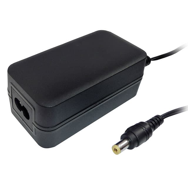
This tutorial walks through designing a compact, regulated 5V/1A rail from an Ideal Power Ltd. 25HK-AY-090A266-DH desktop adapter, a 9V/24W AC/DC brick. The adapter is a good teaching vehicle because it is a sealed, safety-approved unit that delivers a clean, isolated 9V DC at up to 2.66A, which means you can focus entirely on downstream regulation and protection rather than mains design. Its barrel-jack output and fixed voltage make it easy to instrument, and the generous current headroom (24W) leaves margin for inrush and transient loads. The goal is a robust 5V rail suitable for a small embedded board or sensor hub, with input protection and clear test points.
Design requirements. Input: 9V DC nominal from the adapter (accept 8.5-9.5V). Output: 5.0V +/-3% at 0-1.0A continuous, 1.5A peak for 100ms. Ripple: under 50mV p-p. Efficiency target: above 80% at full load. Protection: reverse-polarity, input overcurrent, output short-circuit, and thermal shutdown. Form factor: single-sided PCB under 40x30mm. The design must be testable with a bench multimeter and a scope without desoldering parts.
Step 1: topology and regulator choice. A linear regulator from 9V to 5V at 1A dissipates (9-5)*1 = 4W, which is impractical in a small enclosure. Use a synchronous buck converter instead. Pick an IC rated for at least 2A and 18V input, such as a 2A, 500kHz synchronous buck in an SO-8 or SOT-23-6 package. The higher switching frequency keeps the inductor small; 500kHz is a good trade-off for EMI and efficiency at this power level.
Step 2: inductor and duty cycle. Duty cycle D = Vout/Vin = 5/9 = 0.556. For a 2A buck with 30% ripple current, delta-I = 0.6A. Inductance L = (Vin - Vout) D / (f delta-I) = (9-5) 0.556 / (500k 0.6) = 7.4uH. Choose a 10uH shielded inductor rated for at least 3A saturation. Its slightly higher inductance lowers ripple and improves light-load behavior.
Step 3: output capacitor. Output ripple from capacitance is delta-V = delta-I / (8 f Cout). For 30mV with 0.6A ripple at 500kHz, Cout = 0.6 / (8 500k 0.03) = 5uF. Use two 22uF ceramic capacitors in parallel to cover ESR and transient response; ceramics have low ESR and are stable with most buck ICs. Add a 100nF bypass at the load connector.
Step 4: feedback divider. With a 0.8V reference, choose R1 (top) = 52.3k and R2 (bottom) = 10k: Vout = 0.8 * (1 + 52.3/10) = 4.98V. Use 1% resistors. Verify the IC's recommended divider range before finalizing.
Step 5: input protection. Add a Schottky diode in series with the input for reverse-polarity protection (e.g., 2A, 40V). Its 0.3V drop costs little at 9V. Add a 1A polyfuse and a 10uF/25V ceramic input capacitor close to the IC. A TVS diode (SMAJ12A) clamps adapter transients.
Component selection rationale. The buck IC should have integrated FETs to save space and a fixed 500kHz frequency to simplify loop compensation. The inductor must be shielded to limit radiated EMI near the barrel jack. Ceramic capacitors avoid the ESR aging of electrolytics and keep the board short. The polyfuse protects against a shorted output without nuisance trips at 1A. The Schottky must be rated above the 2.66A adapter limit to survive a fault. A small LED plus 1k resistor on the 5V rail gives a visual power indicator.
Simulation tips. Model the adapter as an ideal 9V source with 0.2 ohm series resistance to represent cable drop. Run a transient simulation with a 1A load step (10-90% in 100us) and check overshoot stays under 100mV. Sweep input from 8.5V to 9.5V and confirm regulation. Plot inductor current to verify it stays below saturation. Check the feedback node for noise pickup and add a small feedforward capacitor across R1 if phase margin is marginal.
Prototype build and testing. Lay out the buck with a tight input loop: input capacitor, IC, and inductor on one side, ground plane underneath. Keep the feedback trace away from the inductor. Solder the barrel jack to a short pigtail and add labeled test points for Vin, Vout, SW, and GND. First power up with a current-limited bench supply set to 9V/100mA, not the adapter, to catch assembly errors. Then switch to the adapter and load with an electronic load: 0A, 0.5A, 1A, and a 1.5A pulse. Measure ripple with a scope using a short ground spring, not a long clip lead. Check thermal rise on the IC and inductor after 10 minutes at 1A; both should stay under 60C above ambient.
Verification and optimization. Confirm 5.0V +/-3% across the load range and input range. Measure efficiency at 0.5A and 1A; if below 80%, check inductor DCR and switching losses. If ripple exceeds 50mV, add a second output capacitor or a small RC snubber across the switch node. Verify short-circuit recovery by briefly shorting the output through a 0.1 ohm shunt and confirming the IC hiccups or current-limits safely. Finally, run a 24-hour soak at 0.8A and log output voltage drift. The result is a compact, protected 5V supply that fully exploits the adapter's 24W headroom while keeping thermal and EMI margins comfortable.