TCAN1043GDQ1 14SOIC Transceiver Application Note Guide
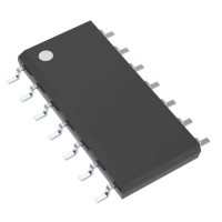
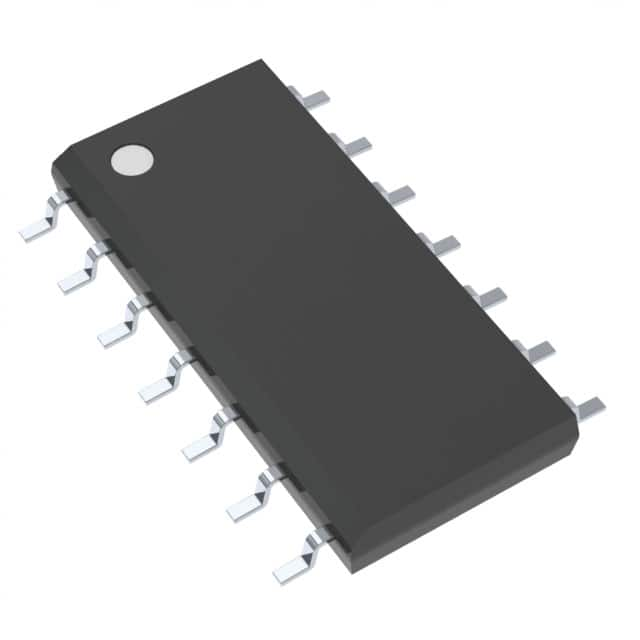
The TCAN1043GDQ1 from Texas Instruments is an automotive-qualified CAN FD transceiver in a 14-pin SOIC package that integrates a high-speed CAN transceiver, a low-dropout (LDO) regulator, and a watchdog/sleep-mode controller, making it well suited for space-constrained, always-on automotive nodes. When integrating this device, start with a topology that reflects its three functional blocks: the CAN bus interface (CANH/CANL), the local power supply (VCC from the battery via VBAT and internal LDO), and the digital control interface (TXD, RXD, EN, INH, and WAKE). The most common and reliable configuration is to power VBAT directly from the vehicle battery rail through a reverse-polarity protection diode or ideal-diode controller, while VCC supplies the local 5 V rail to the microcontroller. Keep the INH output connected to an external high-side switch if you need to control additional loads, and tie EN and WAKE according to your sleep strategy.
For supporting passives, select the VCC decoupling capacitor carefully: a 100 nF X7R ceramic in close proximity to the VCC pin is mandatory for high-frequency transient suppression, and a 4.7 µF to 10 µF bulk capacitor should be placed within a few millimeters to stabilize the internal LDO during load steps. On the bus side, use a split termination network (two 60 Ω resistors with a 4.7 nF to 100 nF capacitor to ground at the midpoint) for improved common-mode rejection, or a single 120 Ω termination at each end of the bus if split termination is not feasible. For ESD and transient protection, the TCAN1043GDQ1 includes integrated IEC 61000-4-2 protection, but adding external TVS diodes (such as a bidirectional 27 V to 36 V standoff device) on CANH and CANL provides an extra margin in harsh environments. Choose the TVS capacitance to be below 30 pF to avoid degrading CAN FD signal integrity at 5 Mbps.
PCB layout is critical for this device because the SOIC package has relatively short lead spacing and the CAN bus is a differential pair. Place the TCAN1043GDQ1 as close as possible to the bus connector, ideally within 10 mm to 15 mm, to minimize stub length. Route CANH and CANL as a tightly coupled differential pair with 100 Ω to 120 Ω differential impedance, matched within 1 mm to 2 mm, and avoid layer changes that introduce impedance discontinuities. Keep the VCC decoupling capacitor on the same layer as the VCC pin with a short, wide trace to ground. The ground pin should connect to a solid ground plane with multiple vias if using a multilayer board. Separate the bus-side ground and the logic-side ground only if your system requires galvanic isolation; otherwise, use a single continuous ground plane to avoid ground-loop issues.
EMC and EMI performance depends heavily on the termination and filtering strategy. The TCAN1043GDQ1 supports CAN FD data rates up to 5 Mbps, so keep the bus stub length below 10 cm and use controlled-impedance traces. For conducted emissions, add a common-mode choke (CMC) in series with CANH and CANL, selecting a part with a differential impedance of 100 Ω to 120 Ω at 100 MHz and a rated current above 100 mA. Place the CMC between the transceiver and the connector, with the termination network on the transceiver side. For radiated emissions, ensure the CANH/CANL traces are routed away from high-speed digital signals and clock lines, and avoid running them parallel to power traces for more than a few millimeters. If the board is in a metal enclosure, bond the connector shield to chassis ground with a low-inductance connection.
Several common pitfalls can degrade performance or cause field failures. First, do not omit the VCC bulk capacitor; the internal LDO can oscillate or drop out during transient loads without it. Second, avoid using a single 120 Ω termination at only one end of the bus; always terminate both ends of the main bus segment. Third, do not connect the INH pin directly to a load without a current-limiting resistor or external switch, as the pin has limited drive capability. Fourth, ensure the WAKE pin is not left floating; use a pull-up or pull-down resistor as specified in the datasheet to define the sleep state. Fifth, verify that the TXD and RXD logic levels match your microcontroller’s I/O voltage; the TCAN1043GDQ1 uses a 5 V VCC, so level shifting may be required for 3.3 V MCUs.
For prototyping and bench testing, start with a simple point-to-point CAN bus between two nodes using 1 m of twisted-pair cable with 120 Ω termination at each end. Measure the differential signal at CANH and CANL with a differential probe to verify the dominant and recessive levels (typically 2 V and 0 V differential). Use a CAN analyzer to confirm communication at 500 kbps and then at 2 Mbps to validate CAN FD operation. Perform a power-up sequence test to ensure the internal LDO stabilizes before the MCU releases reset, and check the INH output timing. For EMC pre-compliance, inject a 1 kHz to 100 MHz sweep into the bus lines using a coupling network and monitor for bit errors. Finally, verify sleep and wake behavior by driving the WAKE pin and measuring current consumption in standby mode, which should be in the microampere range.