MEMS Oscillator Design Tutorial: 12MHz LVCMOS Clock Guide
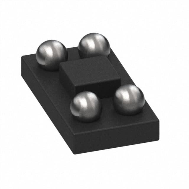
The SiTime SIT8021AI-J4-XXS-12.000000 is a 12 MHz MEMS oscillator in an ultra-small 4-pad package (1.5 × 0.8 mm class footprint), delivering LVCMOS output across a 1.8 V to 3.3 V supply range. Unlike quartz crystals, it contains a complete oscillator — resonator plus driver — so you do not need load capacitors, an external inverter, or careful crystal layout. That makes it ideal for a tutorial: the design is simple enough to complete in one sitting, yet it teaches real skills around supply decoupling, output termination, jitter measurement, and layout. Typical uses include MCU clocking, USB-to-serial bridge references, and low-power sensor nodes where board space and startup reliability matter.
Design requirements. Target a 3.3 V rail with ±5% tolerance, driving a single CMOS clock input (e.g., an STM32 or ESP32 GPIO) at 12 MHz. Required output: LVCMOS, 50% duty cycle nominal, rise/fall times under ~5 ns into a light load. Operating temperature: −40 °C to +85 °C (the "I" suffix indicates industrial grade). Budget: under $2 for the oscillator and passives. The board should fit a 15 × 20 mm area and tolerate a 10–90% supply ramp.
Step 1 — Confirm electrical limits. From the datasheet family, the SIT8021 series draws roughly 3–5 mA at 3.3 V with no load. Check the output drive strength: LVCMOS at 12 MHz into a 15 pF load is well within spec. Verify the enable/disable pin (if present on your exact variant) is tied high through a 10 kΩ resistor to VDD, or left floating per datasheet guidance. If your variant lacks an enable pad, skip this — but always read the specific ordering code's pinout.
Step 2 — Decoupling. Place a 0.1 µF X7R 0402 capacitor within 1–2 mm of the VDD pad, with the return path to a solid ground plane. Add a 1 µF 0603 bulk cap nearby for supply transients. The 0.1 µF handles the oscillator's switching current spikes; the 1 µF smooths rail droop during startup.
Step 3 — Output termination. For short traces (<5 cm) to a high-impedance CMOS input, no series resistor is needed. If the trace exceeds 5 cm or runs near noisy signals, add a 22–33 Ω series resistor at the oscillator output to damp reflections. Calculate the trace impedance roughly as 50–80 Ω for a 6-mil microstrip; the series resistor plus driver impedance should approximate the trace impedance. Do not add a pull-down or load capacitor — LVCMOS drivers are specified into a load, and extra capacitance only slows edges.
Step 4 — Layout. Keep the oscillator away from switching regulators and high-current loops. Route the clock trace as a controlled-impedance line over continuous ground, and avoid stubs. Do not route other signals under the oscillator's pads.
Complete BOM rationale. U1: the SiTime SIT8021 (12 MHz, 3.3 V, industrial). C1: 0.1 µF X7R 0402 (high-frequency decoupling, stable over temperature). C2: 1 µF X5R 0603 (bulk). R1: 10 kΩ 0402 (enable pull-up, if applicable). R2: 33 Ω 0402 (optional series damping). All parts are common, low-cost, and available from multiple distributors.
Simulation tips. In SPICE, model the oscillator as an ideal 12 MHz pulse source with 2 ns rise/fall and 15 pF load to check the receiving IC's input threshold and any ringing. Use an IBIS model if the vendor provides one. Look for overshoot above VDD + 0.3 V and undershoot below −0.3 V at the receiver. Sweep the series resistor from 0 to 47 Ω and observe edge shape. Also simulate the supply ramp: a slow 1 ms ramp with the 1 µF cap should show no startup glitch.
Prototype and test. Build on a two-layer board with a ground plane. Power from a bench supply at 3.3 V with a 100 mA current limit. Probe the output with a 10:1 FET probe (low capacitance) and confirm frequency with a frequency counter: expect within ±20–50 ppm at room temperature. Measure duty cycle and rise/fall times at 10–90%. Check current draw: ~4 mA expected. Verify startup time from power-on to stable clock — typically under 5 ms.
Verification and optimization. Measure phase jitter with an oscilloscope's TIE histogram or a phase-noise analyzer; the SIT8021 family typically delivers sub-1 ps RMS integrated jitter in the 12 kHz–20 MHz band. If jitter is high, inspect decoupling placement and ground continuity. Test at −40 °C and +85 °C if possible; MEMS devices are notably stable across temperature compared with quartz. Optimize by shortening the clock trace and, if EMI is a concern, increasing the series resistor slightly — but re-check rise time against the receiver's requirement.