LTC6259IDC Op-Amp Design Tutorial: Dual 8DFN Circuit Guide
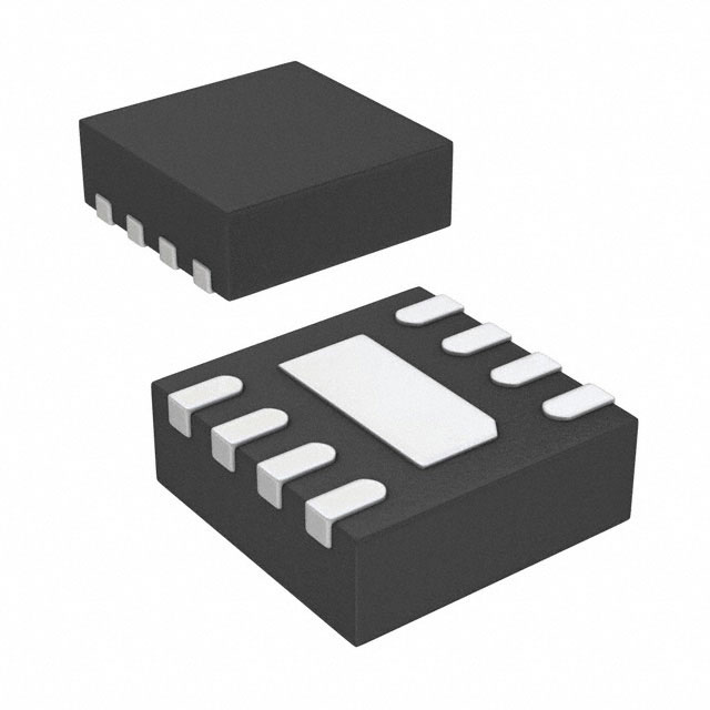
The LTC6259IDC#TRMPBF from Analog Devices is a dual general-purpose operational amplifier in an 8-pin DFN package. It offers rail-to-rail input and output operation, a 4 MHz gain-bandwidth product, and a low supply current of roughly 55 µA per amplifier, making it an excellent choice for battery-powered signal conditioning. Its DFN package with exposed pad provides good thermal performance and a compact footprint. For this tutorial we will design a dual-channel, low-power photodiode transimpedance amplifier followed by a gain stage, a common building block in portable optical sensing. The LTC6259’s low input bias current and rail-to-rail output make it well suited to this task.
Design requirements: Supply voltage 3.3 V single-ended. Photodiode capacitance 10 pF, responsivity 0.5 A/W. Target transimpedance gain 1 MΩ, bandwidth at least 50 kHz, output swing 0.1 V to 3.2 V. Second stage non-inverting gain of 5 V/V. Total quiescent current below 200 µA. Operating temperature 0–70 °C.
Step 1 — Transimpedance stage. Choose feedback resistor Rf = 1 MΩ. The feedback capacitor Cf sets stability and bandwidth. The pole formed by Rf and the total input capacitance Cin (photodiode plus op-amp input, about 12 pF) is f_p = 1/(2π Rf Cin) ≈ 13.3 kHz. To ensure a phase margin of at least 45°, set Cf so the feedback pole is at least the geometric mean of f_p and the gain-bandwidth product (4 MHz). A practical value is Cf = 4.7 pF, giving a closed-loop bandwidth of about 34 kHz, close to the target. If more bandwidth is needed, reduce Rf to 470 kΩ and increase the second-stage gain.
Step 2 — Second stage. Configure the second op-amp as a non-inverting amplifier with gain 1 + R2/R1 = 5. Choose R1 = 10 kΩ, R2 = 40.2 kΩ (standard 1% value). Add a 100 pF capacitor across R2 to limit high-frequency noise and prevent ringing. The overall transimpedance becomes 5 MΩ.
Step 3 — Biasing and decoupling. Use a 0.1 µF X7R ceramic capacitor at each supply pin plus a 10 µF tantalum or ceramic bulk capacitor near the package. The DFN exposed pad must be soldered to a ground plane for thermal and noise performance.
BOM rationale: The LTC6259IDC#TRMPBF is the core amplifier. Rf = 1 MΩ, 0.1% thin-film for low drift. Cf = 4.7 pF C0G for stability. R1 = 10 kΩ and R2 = 40.2 kΩ, 1% metal film. Decoupling: 2 × 0.1 µF 0603 X7R, 1 × 10 µF 0805. A 3.3 V LDO such as the ADP7142 provides a clean supply. All passives are chosen for low thermal noise and tight tolerance.
Simulation tips: Build the circuit in LTspice, which includes the LTC6259 model. Use a photodiode model as a current source in parallel with 10 pF. Run an AC sweep from 1 Hz to 10 MHz and check the transimpedance gain flatness and phase margin (aim for >45°). Perform a transient run with a 10 µA pulse to verify settling and output swing. Add a noise analysis; the dominant noise should come from Rf. Watch for peaking near 30–50 kHz, which indicates insufficient Cf.
Prototype build: Use a small two-layer PCB with a solid ground plane. Keep the photodiode trace short and guard it with ground. Solder the DFN with hot air or reflow; verify continuity on the exposed pad. Power the board from a bench supply at 3.3 V through a 100 Ω series resistor to catch excessive current. First measure the DC output with no light; it should sit near mid-supply if you add a bias network, or near 0 V in this inverting configuration. Then illuminate the photodiode with a modulated LED and observe the output on an oscilloscope.
Verification and optimization: Sweep the LED modulation frequency from 1 kHz to 200 kHz and record the output amplitude to plot the frequency response. Compare with simulation. Measure input-referred noise with a spectrum analyzer or a low-noise scope. If bandwidth is low, reduce Cf to 3.3 pF; if ringing appears, increase Cf. Check quiescent current with a µA meter; it should be under 200 µA. For best performance, shield the photodiode from ambient light and use a metal enclosure. Finally, verify output swing at both rails by increasing the LED drive until clipping occurs, and confirm that the LTC6259 recovers cleanly.