SMD Wire-Wound Ferrite Core Inductor CT1008LSCF-R15J Application Guide
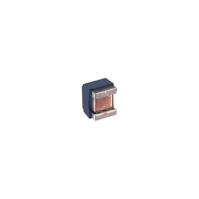
The Central Technologies CT1008LSCF-R15J is a 1008-size (2.5 mm × 2.0 mm) wire-wound ferrite-core inductor with a nominal inductance of 0.15 µH and a "J" tolerance of ±5%. Its ferrite core and wire-wound construction give it relatively high Q and low DC resistance for its footprint, making it well suited to RF and power-conversion roles where efficiency and signal integrity matter. Typical applications include impedance matching networks, RF chokes and bias feeds, low-pass and band-pass filters, EMI suppression in DC-DC converter outputs, and resonant tanks in low-power switching supplies. Treat it as a general-purpose RF/power inductor, but verify its saturation current and self-resonant frequency against your specific operating conditions before committing to production.
For RF signal paths, this part performs best in impedance matching networks, filter sections, and RF chokes where the signal current is small and the inductor operates well below its self-resonant frequency. Keep the working frequency comfortably under the SRF—ideally below one-third of it—so the part behaves inductively rather than capacitively. In power applications, use it in buck or boost converters, output filters, and input pi-filters where the DC bias stays within the rated saturation current. Design best practice is to derate: operate at no more than 70–80% of the rated saturation current to avoid inductance roll-off and thermal stress, and account for inductance drop under DC bias when calculating ripple. For filter designs, choose the corner frequency so that component tolerance (±5%) does not push the response outside specification, and simulate with worst-case L values at both tolerance extremes.
Supporting passives deserve careful selection. For the filter and matching capacitors, use low-ESR, high-Q dielectrics such as C0G/NP0 for RF paths; avoid X7R or Y5V in tuned circuits because their voltage and temperature coefficients will detune the network. In power filters, low-ESR ceramic or polymer capacitors are appropriate, but verify their ESR and ripple-current ratings at the switching frequency. For snubbers and damping networks, use resistors with low parasitic inductance and keep lead lengths short. If the inductor sits in a bias-tee or RF choke role, the decoupling capacitor on the supply side should be large enough to present a low impedance at the operating frequency while not creating an unintended resonance with the inductor; check the parallel resonance of the L-C pair. Select all passives with tolerances and temperature ratings that match or exceed the inductor's, so the overall circuit drift is dominated by the tightest component.
PCB layout is critical for a wire-wound ferrite inductor. Place the part as close as possible to the active device it serves, and keep the current loop area small by routing the return path directly beneath or adjacent to the inductor's traces. For RF use, keep the ground plane continuous under the inductor but avoid running sensitive traces directly beneath it, since the ferrite core concentrates magnetic flux and can couple into nearby traces. Orient the inductor so its axis is perpendicular to adjacent inductors or transformers to minimize mutual coupling; when two inductors must sit near each other, separate them by at least one component body width and rotate one 90 degrees. Use short, wide traces for power paths to reduce resistive loss and parasitic inductance, and avoid sharp 90-degree bends. In 1008 packages, pad geometry matters: follow the manufacturer's recommended land pattern, keep solder fillets uniform, and avoid placing vias directly in the pad unless they are tented or plugged, since solder wicking can starve the joint.
For EMC and EMI, this inductor is a useful tool but not a cure-all. In DC-DC converters, place it in the output filter with the input and output capacitors close by to form a tight pi network, which suppresses both conducted and radiated emissions. Use a shielded or ground-referenced layout where possible, and keep the switching node trace short and away from the inductor's body to reduce capacitive coupling. The ferrite core provides some inherent high-frequency loss, but do not rely on it alone: add a small series ferrite bead or common-mode choke on cables if radiated emissions are a concern. Be aware that the inductor's parasitic capacitance forms a parallel resonance that can create a high-impedance peak; if this peak aligns with a harmonic of your switching frequency, it can amplify emissions. Measure the SRF and check for resonance peaks during pre-compliance testing, and damp them with a small series resistor or a parallel RC snubber if necessary.
Common pitfalls include exceeding the saturation current and assuming inductance stays constant under load—always consult the L-versus-I curve. Another frequent error is ignoring the self-resonant frequency and using the part above it, where it behaves like a capacitor. Designers also underestimate tolerance stack-up: a ±5% inductor combined with ±10% capacitors can shift a filter corner by 15% or more. Poor pad layout causing tombstoning or insufficient solder fillets is a manufacturing pitfall, especially on small 1008 bodies. Finally, placing the inductor near a heat source can shift its ferrite properties; keep it away from power resistors and regulators.
For prototyping, build the circuit on a board that mimics the final layout as closely as possible, including ground planes and trace widths. Measure inductance and Q with an impedance analyzer or LCR meter at the actual operating frequency, not at 1 kHz. Use a network analyzer to check the filter or matching response and compare against simulation. For power designs, run the converter at nominal and worst-case load, measure ripple and efficiency, and use a current probe to confirm peak inductor current stays below saturation. Perform a thermal check with an infrared camera or thermocouples after 30 minutes at full load. Finally, do a quick pre-compliance scan for radiated and conducted emissions before committing to production tooling.