BRL3225T3R3M Application Note: 3.3µH SMD Inductor Design Guide
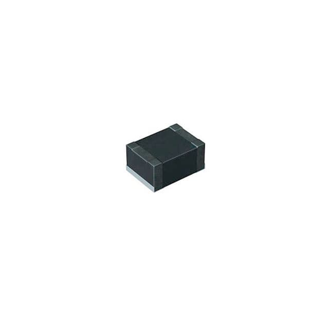
The Taiyo Yuden BRL3225T3R3M is a 3.3 µH wire-wound, magnetically shielded power inductor in a 1210 (3225 metric) package rated for 1.2 A with a maximum DC resistance of 144 mΩ. It is best suited to low-to-medium power DC-DC conversion where board area is tight and radiated field must be controlled. It performs well as the main energy-storage inductor in buck converters operating from 3.3 V, 5 V, or 12 V rails with output currents up to roughly 1 A, and it is a good fit for boost converters and SEPIC topologies in portable and battery-powered products where switching frequencies fall in the 500 kHz to 2.2 MHz range. It is not intended for high-current point-of-load rails, for circuits where saturation current above 1.5 A must be guaranteed, or for high-Q resonant tanks; for those, step up to a larger case size or a different core material. Keep the inductor current ripple in buck designs to 20–40 percent of the DC load current so the peak stays comfortably below the saturation rating across temperature.
Select the input and output capacitors with the inductor's ripple current in mind. Use low-ESR ceramic capacitors (X5R or X7R) for both input and output, sized so the input capacitor sees an RMS ripple current comparable to the inductor ripple and the output capacitor's ESR-zero does not interact badly with the loop. A 10 µF input capacitor and a 22 µF output capacitor are reasonable starting points for a 1 A buck at 1 MHz; verify with the controller vendor's loop tool. For the catch diode in non-synchronous designs, choose a Schottky diode rated at least 1.5× the maximum reverse voltage with low forward drop at the peak inductor current. In synchronous designs, ensure the low-side FET's body diode and dead time are compatible with the inductor's fast current slew. Feedback divider resistors should be 1 percent tolerance or better, and the feedforward capacitor across the top resistor should be tuned to the crossover frequency you actually measure, not just the datasheet suggestion.
Place the inductor close to the switching node and the output capacitor, keeping the high-diode-current loop as small as possible. The loop formed by the input capacitor, high-side switch, inductor, and output capacitor should be compact and on one layer if possible, with a solid ground plane directly beneath it. Route the switch node on a short, wide trace; it is a high-dv/dt node and should be treated as an antenna, so keep its copper area modest. Do not route sensitive feedback or enable traces under or adjacent to the inductor, and keep them away from the switch node. The BRL3225T3R3M is magnetically shielded, but its shield is not perfect; keep it at least 2–3 mm from precision analog circuitry and from any unshielded inductors. Provide thermal relief on the pads consistent with your reflow profile, and follow the manufacturer's recommended land pattern rather than a generic 1210 footprint, since pad geometry affects both solder joint reliability and effective DCR.
Because the part is shielded, most of its EMI contribution comes from the switching node and the loop, not the inductor body itself. Still, the inductor's winding capacitance can couple high-frequency ringing into nearby traces, so add a small RC snubber across the switch node to ground if ringing is excessive. Keep the ground plane continuous under the converter and stitch it generously to any adjacent ground layers. If the design must meet conducted emissions limits, add a small common-mode choke or ferrite bead on the input leads and verify with a LISN measurement. For radiated emissions, the switch node copper area, loop area, and cable routing usually dominate; the shielded inductor helps, but do not rely on it alone. Place the converter away from board edges and connectors where cables can act as antennas.
A frequent mistake is selecting this inductor on nominal current alone and ignoring the saturation current at the maximum ambient temperature. Check the datasheet curves: inductance falls as DC bias rises, and a 1.2 A rated part may saturate well before that at elevated temperature, causing excessive ripple, poor regulation, and audible or electrical instability. Another common error is using a generic 1210 land pattern that leaves the part slightly misaligned, which raises DCR and can crack the winding during thermal cycling. Also avoid placing the inductor directly over a ground-plane cutout or a via array, which changes its effective inductance and can worsen EMI. Finally, do not assume the 144 mΩ DCR is worst case at your operating temperature; copper resistance rises with temperature, so budget for conduction loss at hot conditions when calculating efficiency and thermal margin.
For prototyping, build the first board with the inductor footprint accessible so you can swap values, and bring out the switch node with a short, low-inductance probe point rather than a long wire. Measure inductor current with a current probe or a small series shunt, not by inferring from output ripple alone. Bench test at the intended input voltage extremes and at no load, half load, and full load, checking for stable switching, acceptable ripple, and no subharmonic oscillation. Sweep the load quickly to observe transient response and check that the inductor current does not overshoot into saturation during load steps. Run a thermal soak at full load in the intended enclosure and verify the inductor case temperature stays within the manufacturer's rating with margin. Finally, perform a conducted emissions pre-scan early, before layout is frozen, so that any needed snubber or input filter changes can still be accommodated.