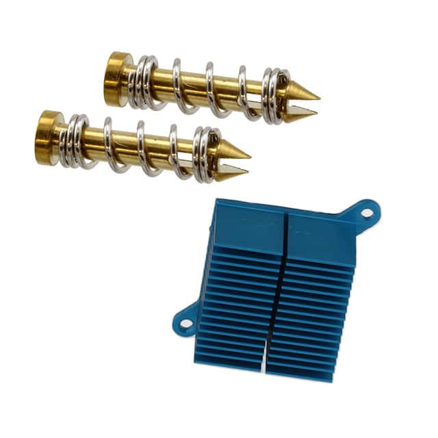
HEATSINK 35X35X25MM R-TAB T766 Application Note: Thermal Design Guide
The ATS-01A-88-C2-R0 is a 35 x 35 x 25 mm extruded aluminum heatsink with an integrated R-tab (screw-and-clip) mounting interface, intended for thermal management of surface-mount power components such as MOSFETs, IGBTs, linear regulators, and stepper driver ICs in the 1 W to 15 W dissipation class. Because the heatsink is a passive thermal component, "circuit topology" here means the thermal network: the die-to-ambient path of junction, package, thermal interface material, and heatsink. The most reliable topology places the device in intimate contact with the heatsink base through a thin, uniform interface layer, with the R-tab providing mechanical retention and a controlled mounting force. Use a single thermal interface material of known thickness and thermal conductivity (typically 0.2 to 0.5 mm, 1 to 6 W/m-K) rather than stacking multiple layers, since each layer adds contact resistance. For multi-device assemblies, avoid sharing one heatsink among devices at very different potentials unless you provide adequate electrical isolation; the anodized finish on this part is not a guaranteed dielectric, so use an insulating pad rated for the working voltage if isolation is required.
Supporting passives should be selected around the thermal and mechanical realities of the package. Gate resistors and decoupling capacitors must be rated for the elevated local ambient (often 20 to 40 °C above board ambient), so derate electrolytics aggressively or replace them with ceramics or polymers near the heatsink. Keep bulk capacitance and any temperature-sensitive references physically away from the heatsink footprint, ideally on the opposite board side or beyond a 10 mm keepout. Choose mounting hardware with a defined torque (typically 0.4 to 0.6 N·m for M3 hardware) and use a Belleville or split washer to maintain clamp force through thermal cycling. If the R-tab is used with a clip, verify the clip force against the device package height tolerance; an oversized gap will defeat the interface material.
PCB layout should treat the heatsink as a mechanical as well as electrical object. Provide a copper keepout matching the 35 x 35 mm footprint plus at least 2 mm clearance for tooling and airflow, and place the heatsink so its fins run parallel to the dominant airflow direction. Route high-current traces directly under the device pad and keep the thermal pad copper pour continuous, avoiding thermal-relief spokes that raise spreading resistance. If the R-tab is soldered or screwed to a grounded pad, define that net explicitly in the schematic so the heatsink is not an accidental antenna. Keep signal traces and sensitive analog nodes at least 3 to 5 mm from the mounting hardware and away from the fin edges, where vibration and creepage are concerns.
From an EMC standpoint, a metal heatsink is a parasitic capacitor and, at higher frequencies, a radiating element. Bond the heatsink to a quiet reference (chassis or local ground) at a single point unless the design explicitly requires a floating heatsink; a single-point bond avoids ground loops while shunting common-mode currents. If the heatsink sits over a switching node, expect increased capacitive coupling and consider a grounded shield or a grounded interposer. Keep the loop area of the device's source/drain and gate return paths small, and place the gate driver close to the device to minimize the antenna formed by long gate traces. Where the heatsink is bonded, use a short, wide strap rather than a long thin wire to keep the bond inductance low.
Common pitfalls include over-torquing the R-tab and cracking the package or the PCB pad, applying too much interface material so it extrudes and shorts adjacent pins, and assuming the heatsink's thermal resistance is independent of airflow. Always derate the published thermal resistance for the actual mounting orientation and airflow; natural convection in a closed enclosure can double the effective value. Another frequent error is neglecting the PCB as a heat spreader: a small pad under the device without copper spreading will bottleneck the path. Finally, do not mount the heatsink over vias that carry signals, since the mounting force can damage via barrels.
For prototyping, start with a thermal mockup: mount the device on a representative board, apply the intended interface material, and measure case temperature with a fine thermocouple or IR camera at the rated load. Run a step-load test and log junction temperature via a built-in diode or a calibrated thermal test die. Verify the mounting force with a torque wrench and inspect the interface imprint after disassembly to confirm full coverage. Bench-test EMC with a near-field probe before and after bonding the heatsink, and repeat the thermal test after 100 thermal cycles to confirm the interface has not degraded. Document the final torque, interface material, and airflow conditions so production and field service can reproduce them.
HEATSINK 35X35X25MM R-TAB T766
Advanced Thermal Solutions Inc. | ATS-01A-88-C2-R0 | $6.52