Design Guide for MEMS OSC VCXO 445.5000MHZ LVDS SIT3373
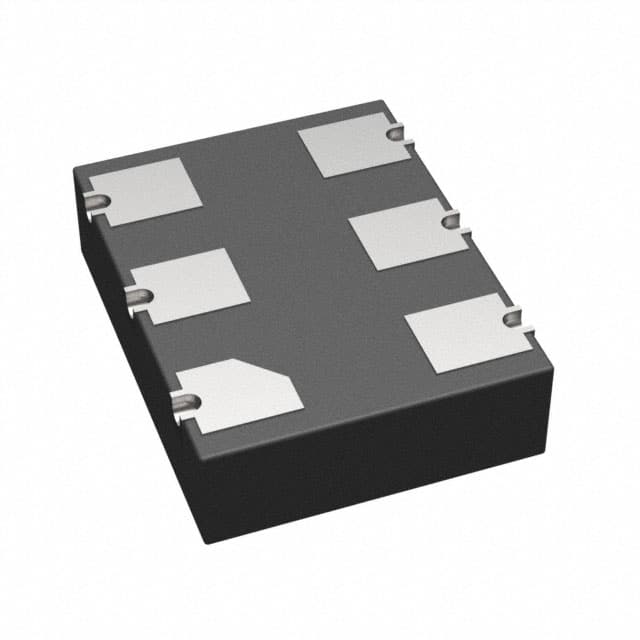
The SiTime SIT3373AC-2B9-30NH445.500000 is a MEMS-based voltage-controlled oscillator (VCXO) delivering a fixed 445.5000 MHz LVDS output. Unlike quartz VCXOs, its silicon MEMS resonator is hermetically sealed and fabricated with semiconductor processes, giving it excellent shock resistance, fast startup, and low sensitivity to board stress. For this tutorial, the part is ideal because it exposes every discipline a clock-tree designer needs: differential termination, supply decoupling, control-voltage filtering, and phase-noise verification. Its 445.5 MHz rate is high enough that layout and termination actually matter, yet low enough to probe with ordinary lab equipment.
Design requirements. Target a clock source for a high-speed serial link (or FPGA reference) that needs 445.5 MHz LVDS, ±50 ppm absolute accuracy, less than 1 ps RMS integrated jitter from 12 kHz to 20 MHz, and a 3.3 V rail. Pull range should cover at least ±100 ppm for fine frequency trim, driven by a 0–3.3 V control voltage. Operating temperature is 0 to 70 °C for the bench prototype. The board is a four-layer FR-4 stackup: signal, ground, power, signal.
Step 1: confirm supply and output levels. The “-30” suffix denotes a 3.0 V nominal supply, so operate from a clean 3.0 V rail (3.0 V ±5% is safe). LVDS outputs are internally biased and expect a 100 Ω differential termination at the receiver. Do not add pull-ups or pull-downs to the output pins; terminate only.
Step 2: decoupling. Place a 0.1 µF X7R capacitor within 2 mm of VDD, plus a 1 µF and a 10 µF bulk capacitor nearby. Keep the return path directly under the part with no plane splits. A small series ferrite bead (600 Ω at 100 MHz) between the bulk rail and the local 0.1 µF is optional but helps isolate switching noise from the rest of the board.
Step 3: control-voltage network. The VCONTROL pin is high impedance. Drive it from a low-noise DAC or a resistor divider from a clean reference. Add an RC low-pass filter, for example 10 kΩ and 0.1 µF, giving a corner near 160 Hz to reject DAC noise. Calculate pull sensitivity from the datasheet: if the specified pull range is ±100 ppm over 0–3.0 V, then sensitivity is about 66.7 ppm/V, so 1 mV of control noise produces roughly 0.067 ppm of frequency error—small, but keep the filter anyway.
Step 4: termination and routing. Route the differential pair as 100 Ω differential impedance, matched within 0.5 mm, with minimal vias. Place the 100 Ω termination resistor at the receiver end. If the receiver is far away, consider AC coupling only if the receiver supports it; LVDS is DC-coupled by default.
Step 5: enable and layout. Tie the enable pin high through a 10 kΩ resistor so the part defaults on, and provide a test point. Keep the oscillator away from switching regulators and clock the ground plane continuously beneath the differential pair.
BOM rationale. The oscillator is the only active device. Choose a 0.1 µF 0402 X7R for low ESL, a 1 µF 0603 X7R, and a 10 µF 0805 X5R for bulk. Use 1% thin-film resistors for the control filter and termination to keep tolerance tight. A 600 Ω ferrite bead and a 10 kΩ enable pull-up complete the set. All parts are standard and inexpensive, keeping the prototype reproducible.
Simulation tips. Run a transient simulation of the control filter to confirm settling time and ripple. Use an IBIS model of the LVDS driver into a 100 Ω load to check differential swing and common-mode voltage at the receiver. In a frequency-domain view, verify the filter corner and look for any resonance with the bulk capacitance. Watch for excessive overshoot on the enable pin if it is driven by a slow ramp.
Prototype build and test. Assemble on the four-layer board, then power the rail and measure VDD ripple with a 1 GHz probe and short ground spring. Verify the output with a differential probe or a 100 Ω feed-through terminator into a scope. Measure frequency with a counter, then sweep the control voltage from 0 to 3.0 V and record frequency versus voltage to confirm pull range and linearity. Measure phase noise with a signal-source analyzer or a phase-noise analyzer, integrating from 12 kHz to 20 MHz.
Verification and optimization. Compare measured jitter to the 1 ps RMS target. If jitter is high, inspect the supply for switching spurs and improve decoupling or add the ferrite bead. Check common-mode noise on the differential pair; poor termination or a split return path is the usual culprit. Temperature-cycle the board to confirm frequency stability. Finally, document the control-voltage slope and the measured phase noise so the next design can reuse the block with confidence.