AD977BRZ Datasheet Guide: 16-Bit SAR ADC IC Explained
The AD977BRZ is a 16-bit, 100 kSPS successive-approximation-register (SAR) analog-to-digital converter from Analog Devices, housed in a 20-lead SOIC (R-20) package. Interpreting its datasheet correctly begins with the resolution and throughput pair: 16 bits at 100 kSPS means an LSB of 153 µV on a 10 V full-scale input, so the converter is aimed at high-accuracy, medium-speed instrumentation rather than high-throughput signal chains. Key static specifications include integral nonlinearity (INL) of ±2 LSB typical and differential nonlinearity (DNL) specified to guarantee no missing codes over the full operating temperature range — the latter matters because a 16-bit SAR must be monotonic to be useful in closed-loop control and weigh-scale applications. Offset and gain errors are factory-trimmed but remain temperature-dependent, so budget for system-level calibration or periodic autozero routines in designs that must hold accuracy across −40 °C to +85 °C.
The dynamic specifications deserve equal attention. SINAD and THD are typically quoted for a 10 kHz input at 100 kSPS; the effective number of bits derived from SINAD is the number to compare against your accuracy budget, not the nominal 16 bits. The input structure is a switched-capacitor track-and-hold, which means the source impedance and acquisition time interact directly: the datasheet's recommended driver amplifier and RC anti-alias network are not optional suggestions but part of the specified performance envelope. The internal reference is a 2.5 V bandgap with its own drift and noise contribution; many precision designs instead drive REF with an external reference, and the datasheet's reference input impedance and settling requirements must be respected if you do so.
Absolute maximum ratings define the boundary between specified operation and permanent damage. The analog inputs are typically limited to the supply rails plus 0.3 V, and the digital inputs likewise; exceeding these, even transiently during power sequencing, forward-biases internal ESD structures and can latch the device. Note that absolute maximum ratings are not operating conditions — the recommended operating range, generally VDD of 5 V ±5% and VCC of 5 V ±5% for this dual-supply part, is where all specifications hold. Derating considerations center on the digital interface: the AD977 is a 5 V-only device with no separate logic supply, so interfacing to 3.3 V FPGAs requires level shifting on the data bus and control lines. Power-supply sequencing should bring up the analog supply before or with the digital supply, and the datasheet's caution against allowing any input to exceed the supplies during power-up should drive your board-level sequencing and protection design.
The typical application circuit is a classic precision SAR front end. An input buffer (the datasheet suggests a low-noise, fast-settling op amp such as the AD797 or OP1177 depending on source impedance) drives the analog input through a small series resistor and a charge-reservoir capacitor to ground; this network absorbs the track-and-hold's switched-capacitor kickback and sets the acquisition settling. The reference pin sees a low-ESR bypass capacitor plus, for external references, a buffer. Supply pins require 0.1 µF ceramic decoupling at the package plus bulk capacitance nearby, and the analog and digital grounds should be joined at a single point under the converter. The conversion start signal (CONVST) and the read interface (CS, RD, and the 16-bit parallel data bus) should be routed away from the analog front end; the parallel bus is fast enough that crosstalk into the input network is a real concern on dense boards.
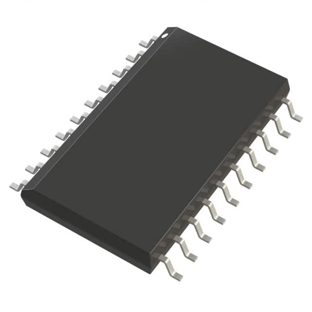
Pin configuration in the 20-lead SOIC follows the standard AD977 family arrangement: analog inputs, reference, supplies, and the parallel interface distributed around the package. Pay attention to the pinout's asymmetry — the analog pins cluster on one side and the digital bus on the other, which is a deliberate layout aid. Keep the analog input traces short and guarded by ground pour, and avoid routing the data bus beneath the input network. The SOIC package's lead frame offers modest thermal performance; the part dissipates well under 100 mW, so thermal management is rarely a limiting factor, but the datasheet's θJA figure (on the order of 75–90 °C/W for the 20-lead SOIC) is useful when the converter sits in a hot enclosure. Ensure adequate copper at the ground pins and avoid stacking the part directly against heat-generating regulators.
Timing diagrams are where many designs fail. Read the conversion timing as a sequence of hard constraints: the CONVST pulse width, the acquisition time before conversion, and the conversion time itself (approximately 10 µs at 100 kSPS) must all be met, and the data-ready or BUSY handshake must be respected before reading. The parallel read cycle has its own address-access and data-valid times; driving CS and RD faster than specified produces stale or invalid data that looks like noise. On the characteristic curves, focus on SINAD and INL versus input frequency and temperature — the curves show where performance degrades, typically at higher input frequencies and temperature extremes, and they should be read as envelopes, not typical-case marketing figures. When specifying the part for purchase, confirm the BRZ grade's temperature range and package marking against the datasheet's ordering guide, and treat any distributor stock that cannot be traced to the AD977BRZ ordering code with suspicion.