MEMS VCXO 153.6MHz LVPECL Datasheet Guide: SIT3372AC Explained
Decoding the SiTime SIT3372AC-1E3-25NU153.600000 part number is itself instructive: it identifies a SiT3372 series differential VCXO in a 7.0 x 5.0 mm package, industrial temperature grade, 2.5 V supply, with 153.600000 MHz output and LVPECL signaling. The device belongs to SiTime's third-generation Elite Platform, built on a programmable MEMS resonator rather than a quartz blank, which yields immunity to shock and vibration and typically ±10 ppb/°C frequency stability with the integrated temperature compensation. For the design engineer, the LVPECL output is the defining datasheet parameter: the datasheet specifies output swing as a differential voltage referenced to VDD, typically 800 mV single-ended into 50 Ω to VDD−2 V, and the driver expects standard 50 Ω pull-down terminations to VDD−2 V or the Thevenin-equivalent network. The 153.600 MHz frequency is a common Ethernet/OTN line-rate multiple, so jitter is usually the selection driver; the datasheet's phase jitter figure (typically 0.2–0.4 ps RMS integrated 12 kHz–20 MHz) should be read as an RMS value over that specific band, not a peak-to-peak number.
Absolute maximum ratings deserve careful reading because VCXO parts are frequently damaged by supply sequencing and by over-driving the control voltage input. The datasheet typically lists VDD absolute maximum around 3.0 V for the 2.5 V option (the 25 in the part number denotes 2.5 V), with a corresponding maximum on the VC control pin near VDD + 0.3 V and storage temperature range of −65 °C to +150 °C. Derating is not optional: operating at 2.5 V ±5% (±125 mV) is the specified condition, and pushing the supply above that increases core power dissipation and can shift output levels outside the LVPECL common-mode window. Note that the industrial temperature range (−40 °C to +85 °C) is an operating range, not a warranty to run at the extremes continuously; junction temperature limits and thermal derating should be applied as described below.
The typical application circuit is straightforward but unforgiving of layout shortcuts. The VDD pin requires a 0.1 µF decoupling capacitor placed within a few millimeters, plus a 10 µF bulk capacitor shared with the local rail. Because LVPECL outputs are open-emitter, each output must be terminated with a 50 Ω resistor to VDD − 2 V, or with a Thevenin split of 50 Ω to VDD and 50 Ω to ground at the receiver, or by AC-coupling into a receiver with internal bias. The VC control input is a high-impedance analog node and should be driven from a low-noise reference; a 0.1 µF bypass to ground at the pin filters reference noise but must not be so large that it slows loop response in a PLL application. The datasheet's pull range (commonly ±50 ppm or ±100 ppm) and linearity specification define the usable tuning window; the transfer function is monotonic but characterized only over the specified VC range, so operation outside that range is unspecified even if the part still oscillates.
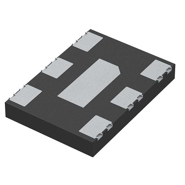
Pin configuration follows the standard 6-pin differential oscillator footprint: pin 1 is the output enable or standby (with internal pull-up, so the device defaults to enabled), pin 2 is the control voltage input, pins 3 and 4 are the differential outputs, pin 5 is VDD, and pin 6 is ground, with the package pad orientation confirmed against the datasheet's top view. The 7 x 5 mm package uses a 4-pad or 6-pad land pattern; the datasheet's recommended land pattern should be copied exactly, and the exposed center pad, where present, is a thermal and ground connection rather than an electrical signal. Because the part is a MEMS device, the package is hermetic and the resonator is not exposed, but the PCB footprint still needs a solid ground plane beneath the device to control return currents from the LVPECL edges.
Thermal management is less about continuous dissipation than about local heating. The device draws roughly 60–80 mA at 2.5 V with both LVPECL outputs terminated, so power dissipation is on the order of 150–200 mW, and the 7 x 5 mm package has a thermal resistance high enough that a poorly ventilated enclosure can raise the die temperature well above ambient. The frequency stability specification is referenced to the die temperature, so placing the oscillator near a hot ASIC or regulator directly degrades the ppm budget; keep it away from heat sources and provide thermal vias to the ground plane. The datasheet's stability-versus-temperature curve is a typical characterization, not a guaranteed envelope, and the ±20 ppm or ±25 ppm limits are guaranteed over the industrial range only when the device is operated within the specified supply and load conditions.
Timing diagrams and characteristic curves should be read literally. The output waveform diagram defines the 20%/80% rise and fall times (typically 300–500 ps for LVPECL) and the differential crossing point; the datasheet's duty cycle specification (often 45–55%) applies at the crossing, so a receiver with a high-sensitivity threshold will see a different effective duty cycle. The phase noise plot is single-sideband, referenced to the carrier, and is the most useful selection curve: it shows the 1/f region and the noise floor, and integrating it over the receiver's bandwidth reproduces the jitter figure. The frequency-versus-control-voltage curve defines the pull range and the slope (ppm/V), which sets the loop gain in a PLL design. Finally, the startup and enable timing diagrams specify the time from power-on or enable release to valid output (often a few milliseconds), which matters for systems that gate clocks during power sequencing. Treat every curve as measured under the datasheet's stated test conditions, and reproduce those conditions in your own characterization.