RSR025P03TL Datasheet: MOSFET P-CH 30V 2.5A TSMT3 Guide
The Rohm Semiconductor RSR025P03TL is a P-channel power MOSFET housed in a compact TSMT3 package, designed for load switching and power management applications where space is at a premium. This device is rated for a maximum drain-source voltage of -30V and a continuous drain current of -2.5A, making it suitable for battery protection circuits, DC/DC converters, and peripheral power distribution in portable electronics. The key electrical specifications begin with the drain-source on-resistance, which is typically 0.145 ohms at a gate-source voltage of -10V, rising to 0.250 ohms at -4.5V. This RDS(on) value is critical for determining conduction losses in your design; lower resistance translates directly to less heat generation and higher efficiency, particularly in high-current paths. The threshold voltage, Vgs(th), is specified between -1.0V and -2.5V, meaning the MOSFET begins to conduct when the gate voltage is more negative than this range. This is important for low-voltage drive circuits, as a logic-level gate signal of 2.5V or 3.3V may struggle to fully enhance the device if the threshold is at the higher end of the range. You should always calculate the gate drive voltage margin relative to the worst-case threshold to ensure the MOSFET operates in its fully enhanced, low-resistance region.
When examining the absolute maximum ratings, the RSR025P03TL can withstand a drain-source voltage of -30V and a gate-source voltage of +/-20V. Exceeding these limits, even momentarily, can cause irreversible breakdown. The maximum continuous drain current is -2.5A at a case temperature of 25°C, but this value must be derated as temperature increases. The datasheet provides a curve showing the current derating factor, which typically reduces the current rating by approximately 0.02A per degree Celsius rise above 25°C. At 100°C, for example, the continuous current may be limited to around 1.5A or less. Pulsed drain current is rated at -10A for a short duration, but this is highly dependent on pulse width and duty cycle, as dictated by the device's safe operating area (SOA) curves. The total power dissipation is specified at 1.0W when mounted on a standard FR4 board, but this rating assumes a specific copper area for heat sinking. In practice, you must derate power based on your actual PCB layout and ambient temperature. The junction-to-ambient thermal resistance, RθJA, is typically around 125°C/W, so a 1W dissipation would raise the junction temperature by 125°C above ambient. For reliable operation, you should keep the junction temperature below 150°C, preferably with a design margin of 20-30°C. This means for a 25°C ambient, the maximum allowable power dissipation is roughly (150-25)/125 = 1.0W, but at 70°C ambient, it drops to (150-70)/125 = 0.64W.
The typical application circuit for this P-channel MOSFET involves connecting the source to the input voltage rail and the drain to the load, with the gate pulled to ground through a resistor to turn the device on. A common configuration is a high-side load switch, where a small NPN transistor or a microcontroller GPIO drives the gate through a series resistor (e.g., 10k ohms) to control the turn-on and turn-off speed. The gate-source resistor (typically 10k-100k ohms) ensures the MOSFET remains off when the drive signal is floating. For inductive loads, such as relays or motors, a flyback diode should be placed across the load to clamp voltage spikes. The datasheet also provides characteristic curves that are essential for understanding dynamic behavior. The output characteristics (Id vs. Vds) show the linear and saturation regions; for a given Vgs, you can determine the drain current at a specific Vds. The transfer characteristics (Id vs. Vgs) help you select the gate drive voltage needed to achieve the desired current. The capacitance curves (Ciss, Crss, Coss) versus Vds are critical for estimating switching losses. Ciss, the input capacitance, influences the gate drive current required for fast switching. The gate charge curve (Qg vs. Vgs) is particularly useful; it shows the total charge needed to turn the device on, and the Miller plateau region indicates where the gate voltage remains constant as the drain voltage switches. To calculate switching times, you can use the gate drive source/sink current and the gate charge values: turn-on time is approximately Qg / Igate.
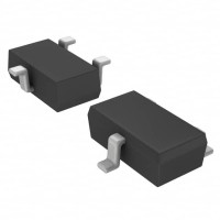
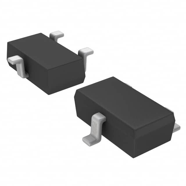
Regarding pin configuration, the TSMT3 package has three leads: pin 1 is the gate, pin 2 is the source, and pin 3 is the drain. The package outline is a surface-mount SOT-23-like footprint, measuring approximately 2.9mm x 2.8mm with a height of 0.8mm. The drain is internally connected to the large tab on the package, which serves as the primary heat path. For thermal management, ensure the PCB copper area connected to the drain pad is as large as possible, ideally with thermal vias to inner or bottom layers. A minimum of 25mm² of copper is recommended for 1W dissipation, but more is better. The thermal impedance can be reduced by using thicker copper and multiple vias. When interpreting the timing diagrams, such as switching time vs. gate resistance, note that the test conditions define the load and gate drive voltage. The datasheet typically shows turn-on delay (td(on)), rise time (tr), turn-off delay (td(off)), and fall time (tf). These are measured at specific Vgs and Id conditions. For example, at Vgs = -10V and Id = -2.5A, the typical turn-on delay is 10ns and the rise time is 15ns. These values scale with gate resistance, so you can use the provided curves to estimate performance for your specific gate drive circuit. Always verify that the switching losses do not exceed the thermal budget, especially at high frequencies. By carefully analyzing these parameters, you can confidently integrate the RSR025P03TL into your design, balancing efficiency, thermal constraints, and switching performance.