Mastering MEMS VCXO Design: 148MHz LVDS Tutorial
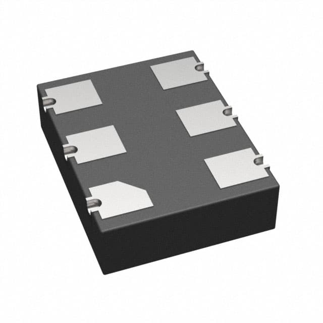
Welcome to this hands-on design tutorial centered around the SiTime SIT3372AI-2B9-33NZ148.351648, a MEMS-based Voltage-Controlled Crystal Oscillator (VCXO). This component is ideal for this tutorial because it combines the precision of a traditional quartz VCXO with the robustness and small footprint of MEMS technology. It delivers a stable 148.351648 MHz LVDS output, making it perfect for high-speed data conversion or FPGA clocking applications. Its wide pull range and low jitter characteristics allow us to explore practical phase-locked loop (PLL) and clock clean-up circuit design without the fragility of quartz.
Design Requirements and Specifications
For this tutorial, we will design a precision clock distribution circuit that takes the VCXO output and fans it out to two high-speed ADC clock inputs. The key requirements are: input voltage of 3.3V (from the VDD spec of the SIT3372), LVDS output swing of 350mV typical, and a control voltage tuning range of 0V to 3.3V to achieve a ±160 ppm pull range. The output must be AC-coupled to the ADCs to handle common-mode differences. We also need to ensure output impedance matching for signal integrity. The design must be compact, using surface-mount components, and the PCB layout must minimize crosstalk.
Step-by-Step Design Process with Calculations
First, calculate the termination resistors. LVDS requires a 100-ohm differential termination at the receiver. For the VCXO's LVDS output, we place a 100-ohm resistor across the differential pair at the far end of the trace. Since we are fanning out to two ADCs, we will use a dedicated LVDS fanout buffer. Choose a buffer like the TI SN65LVDS111 with a 1:2 fanout. The buffer's input impedance is high, so the termination remains at the ADC inputs. Next, determine the coupling capacitors. For AC coupling, use 0.1uF ceramic capacitors in series with each line. The -3dB high-pass cutoff is f = 1/(2πRC). With a 100-ohm termination and 0.1uF, cutoff is about 16 kHz, well below the 148 MHz signal. For the control voltage input, we need a low-pass filter to prevent noise from the tuning source. Use a 10k resistor and a 0.1uF capacitor to ground, giving a cutoff of ~160 Hz. This filters power supply ripple but allows slow modulation for the PLL.
Component Selection Rationale for the Complete BOM
The centerpiece is the SiTime SIT3372AI-2B9-33NZ148.351648, chosen for its low jitter (0.5 ps RMS typical) and wide pull range. For the fanout buffer, the SN65LVDS111 provides low skew (<50 ps) and operates from 3.3V. Use 100-ohm 0603 resistors with 1% tolerance for termination. Coupling capacitors are 0.1uF X7R ceramic (0402 size) for good temperature stability. For the control voltage filter, use a 10k 0603 resistor and a 0.1uF X7R capacitor. Bypass capacitors: 0.1uF and 10uF ceramic in parallel at the VCXO and buffer power pins. A 100-ohm common-mode choke on the LVDS output lines (e.g., Murata DLW21SN) can further reduce common-mode noise. Finally, use a 49.9-ohm resistor to ground on the VCXO's OE pin to enable it if not used.
Simulation Tips and What to Look For
Use an LTspice or HyperLynx simulation to verify signal integrity. Model the VCXO as a 3.3V LVDS source with 350mV swing and 100-ohm output impedance. Place the 100-ohm termination, AC coupling caps, and the fanout buffer. Look for differential voltage swing at the ADC inputs: it should be between 250mV and 450mV. Check for overshoot (should be <10% of swing) and ringing. Simulate the control voltage filter: apply a 100mV step to the control input and observe the VCXO output frequency. The settling time should be under 1ms. Also simulate power supply rejection: inject 100mV ripple at 1MHz on VDD and measure jitter at the output. Expect less than 1 ps added jitter.
Prototype Build and Testing Methodology
Build the circuit on a 4-layer PCB with a dedicated ground plane. Place the VCXO close to the fanout buffer and route the LVDS traces as a differential pair with 100-ohm controlled impedance. Keep trace lengths under 2 inches to minimize loss. Solder all components using reflow or hot air. For initial testing, use a 3.3V bench supply and a function generator for the control voltage (0-3.3V). Connect the output to a high-speed oscilloscope with differential probe (or use a balun). Apply 1.65V to the control pin (center of pull range) and verify the output frequency of 148.351648 MHz within 10 ppm. Then sweep the control voltage from 0 to 3.3V and measure frequency change. It should be ±160 ppm. Connect to the ADCs and verify clock signals at the ADC pins using a scope.
Performance Verification and Optimization
Measure phase noise using a spectrum analyzer with phase noise measurement capability. At 10 kHz offset, expect better than -140 dBc/Hz. Measure jitter with an oscilloscope using jitter measurement software: RMS jitter should be <1 ps. If jitter is high, check power supply cleanliness and add ferrite beads on VDD lines. Optimize the control voltage filter: if tuning noise is present, increase the resistor to 100k and capacitor to 1uF for a lower cutoff. For thermal stability, operate the circuit in an environmental chamber from 0°C to 70°C and verify frequency drift is <50 ppm. Finally, test with the ADCs running at full speed and verify that no bit errors occur. If needed, adjust the control voltage to center the ADC sampling point.
Conclusion
This tutorial has walked you through designing a practical clock distribution circuit using the SiTime SIT3372AI-2B9-33NZ148.351648 MEMS VCXO. You now have the calculations, component choices, simulation steps, and testing methods to build a robust, low-jitter clock source. The MEMS technology offers superior reliability and ease of use compared to quartz, making it an excellent choice for modern high-speed designs.